
Home » Posts tagged 'Vivante'
Tag Archives: Vivante

GCNano GPUs – Supercharging your Wearables and IoT
Vivante recently announced the GCNano GPU Series, the latest product line that complements its shipping Vega GC7000 Series to complete the world’s first full line-up of top to bottom GPU offerings, from the smallest wearables and IoT devices, to ultra HD 4K / 8K TVs, smartphones and tablets. GC7000 targets SoCs that need the latest and greatest GPU hardware and features like OpenGL ES 3.1, Full Android Extension Pack Support, DirectX 12, tessellation / geometry shaders, ray tracing, zero driver overhead and GPGPU for vision / image / physics processing, with the most aggressive PPA and feature-complete design. GCNano falls on the other side of the spectrum without sacrificing features or performance, and targets devices that are making a revolutionary (visual user interfaces / UI, network connected, intelligence) push into consumer products like wearables and IoT (smart homes / appliances, information gadgets, etc.). Many of these new products will be powered by microcontroller (MCU) and microprocessor (MPU) systems that will complement the general purpose applications processors (AP) found in mobile and home entertainment products. (I’ll use the term MCU to collectively reference MCUs and MPUs).
About MCUs
MCUs are task specific “embedded” processing devices that are found in the billions inside everything from the washing machine control / interface and thermostats with displays, to remote controls, network printers with displays, smart meters, and other devices in the home, car, infrastructure or on the body. Most of them are invisible to us, but behind the scene they keep our world moving. Traditional MCUs only supported basic visual interfaces since their focus was to display relevant information and keep things simple. Over the last several years the industry took a sharp turn and evolved to where MCUs where not just data processors but the HMI (human-machine interface) of some consumer devices. Nest thermostats, washing machines with color displays and the next generation health wearables are examples of this shift. As screens become pervasive, demand for fancier UIs that have an intuitive, consumer friendly look-and-feel will be required. GCNano specifically targets these types of systems since an innovative and special type of GPU needs to be used to overcome system and resource constraints, without negatively impacting user experience.
MCUs have limited CPU resources, limited memory resources, limited bandwidth, limited I/O, and require ultra low power (ex. long battery life). Previous products could get by using a simple display controller and CPU (software) or simple 2D engine to create a basic GUI. But as graphics UI complexity increases (layers, content, effects) and resolutions/PPI go up, this method will not suffice since it will overwhelm system resources. To overcome these limitations you cannot take a standard off the shelf GPU IP block and plug it in. You need to examine the constraints and optimize the design for this type of configuration through a holistic approach that includes hardware (GPU, UI-display controller integration), software (drivers, tools, compilers, etc.) and ecosystem enablement.
On the hardware side you are looking at the feature list and elminating unused ones (ex. 3D game features), optimizing PPA, fine-tuning datapaths and memory, enabling compression, reducing bandwidth and creating a tightly coupled interface between the UI / composition GPU and display controller. In addition, removing or significantly reducing external DDR memory cuts system cost dramatically since DDR is a major portion of BOM cost. On the software side you need to look at drastically cutting down driver size, driver overhead, batching calls, compilers (for example, pre-compiled shaders), and creating a standard wearables / IoT GPU SW package that developers can tap into. Having a tiny driver size is critical since you need instantaneous screen response at the push of a button (wearable) or when you start your car and the dashboard information needs to appear in less than a second (IoT). GPUs are complex, powerful and programmable, yet the GCNano takes a simpler approach and takes the guesswork out to keep things relevant and functional.
GCNano Product Overview
The GCNano can be split into two types of products. On one side you have the GCNano Lite which is a vector graphics engine that can render with no-OS and no-DDR memory and is shipping now (production proven). The other category is products that require 3D rendering using OpenGL ES 2.0 (at a minimum) but still need a tiny memory footprint (minimal DDR) and customized / limited / high-level operating systems (GCNano and GCNano Ultra). The table below shows the various products.

GCNano Series benefits include:
- Wearables and IoT Ready: Ultra-lightweight vector graphics (GCNano Lite) and OpenGL ES 2.0 (GCNano, GCNano Ultra) drivers, SDK and tools to easily transition wearables and IoT screens to consumer level graphical interfaces. The GCNano package also includes tutorials, sample code, and documentation to help developers optimize or port their code.
- Designed for MCU/MPU Platforms: Efficient design to offload and significantly reduce system resources including complete UI / composition and display controller integration, minimal CPU overhead, DDR-less and flash memory only configurations, bandwidth modulation, close-to-the-metal GPU drivers, and wearables / IoT-specific GPU features to shrink silicon size. The tiny software code size puts less constraints on memory size, speeds up GPU initialization and boot-up times.
- Ecosystem and Software Support: Developers can take advantage of the lightweight NanoUI or NanoGL API to further enhance or customize their solutions. Large industry support on existing Vivante products include the GCNano / GCNano Ultra product line on Android, Android Wear and embedded UI solutions from key partners covering tools for font, artwork and Qt development environments.
- Compute Ready: As the number of wearable / IoT (processing) nodes grows by several tens of billions of units in the next few years, bandwidth on data networks could be an issue with an always-on, always-connected, always-processing node. GCNano products help with this by performing ultra low-power processing (GFLOP / GINT ops) at the node and only transmits useful compressed data as needed. Examples include sensor fusion calculations and image/video bandwidth reduction.
Vivante’s software driver stack, SDK and toolkit will support its NanoUI API that brings close-to-the-metal GPU acceleration for no-OS / no-DDR options on GCNano Lite and the NanoGL API for more advanced solutions that include proprietary or high-level operating systems like embedded Linux, Tizen™, Android™, Android™ Wear and other RTOS that require OpenGL ES 2.0+ in the smallest memory footprint. These various OS / non-OS platforms will form the base of next generation wearables and IoT that bring personalized, unique and optimized experiences to each person. The GCNano drivers include aggressive power savings, intelligent composition and rendering, and bandwidth modulation that allow OEMs and developers to build rich visual experiences on wearables and IoT using an ultralight UI / composition or 3D graphics driver.
Many of the GCNano innovations create a complete “visual” MCU platform that optimizes PPA and software efficiency to improve overall device performance and BOM cost, with the most compact UI graphics hardware and software footprint that does not diminish or restrict the onscreen user exprience. These new GPUs are making their way into some exciting products that will appear all around you as wearables and IoT get integrated and eventually “dissappear” into our lives.
Android Secure GPU Content Protection
Data and device security play a very important role in today’s always connected lifestyle. The proliferation of devices found at home, at work, in the car, and all around us (i.e IoT) blur the lines between personal, business, and our financial lives. We use our smartphones for ePayments, rent movies on our smart TV, and send secure corporate data from our tablets. While the exponential growth in the number of smart “personal/corporate” devices is great for convenience, it becomes a security nightmare with data explosion in the cloud and across our personal networks. We expect our confidential data to be protected and secure at all times, yet readily accessible anytime, anywhere.
In this blog we will take a different approach to data security and focus on our expertise, showing how to protect data as it travels down the visual processing pipeline through a secure GPU and memory subsystem inside an SoC.
Out of the Box Thinking
To make security even more secure, you need to think outside the box beyond 2-step authentication, encryption, network security, TrustZone, and others. There are great technologies that already cover those parts of security, so the solution developed by Vivante and the Android team takes another approach and is not intended to replace any of the existing protocols. The solution only augments the entire security process to give users even more peace of mind.
One area that we researched was how to keep data processed inside the GPU pipeline and rendered onscreen secure, through a tightly controlled GPU/SoC infrastructure. Historically, GPUs and security have never been used in the same sentence as synonymous technologies. GPUs were only focused on rendering life-like 3D graphics or performing Compute tasks for vision / image processing. Moving forward the industry will take a different approach to GPUs with the introduction of Vivante’s Secure GPU technologies, with the goal to bring GPU security to all mass market Vivante powered Android devices so everyone can benefit. Vivante already gained first-hand experience working on secure GPU solutions with some of our partners, one notable company being Blackberry (formerly known as Research in Motion), famous for their secure solutions used in enterprise and government offices, and other multimedia companies that used the GPU to process protected video content.
We looked for a solution that is truly usable, effective, scalable for future use cases, and economical, so we asked ourselves some questions like:
- Is there any way to secure data to make sure it cannot be accessed by a rogue application?
- What happens to the data that is in the frame buffer (surface) before, during, and after the rendering process? Can we ensure the data is safe and how?
- Can we secure data for graphics, video, images, text, bitmaps, composition surfaces, and more?
- How do you allocate surfaces and make sure secure surfaces reside in memory locations only accessible by secure clients only?
- What happens in virtualization when a Vivante GPU can be virtualized (vGPU) across multiple users and multiple secure/non-secure operating systems (OS) and data needs to be firewalled?
All these questions were catalysts for the creation of a new Khronos EGL extension for the Android OS platform which will be highlighted below. There are parts of the Vivante GPUs architected for security and virtualization that go beyond what is described in this piece, and those will be described in a future blog.
Creation of a Secure GPU
Over the last several months, Vivante had been involved in deep technical discussions with Google’s Android team and Marvell to come up with a watertight solution to stop protected content from falling into the wrong hands. Protected content in this scenario relates to any visual confidential information like numbers, passwords, protected video, secure zones on the user interface (UI), GPU data in system memory and cache, and virtualization of the GPU that splits data between secure and non-secure (general) operating systems (OS).
The solution created is now the latest Khronos Group EGL extension that has become an important piece of the Android OS where they recommend its use. For reference, EGL (Embedded systems Graphics Library) is the main interface between client graphics APIs like OpenGL ES and the native windowing system. The EGL layer handles housekeeping functions like synchronization between threads, context management, memory allocation, binding/unbinding surfaces, and workload distribution between different rendering APIs.
Overview of the EGL Extension
In single and multi-OS environments, there are two types of memory/buffer accesses and copy functions, namely secure and non-secure. Non-secure accesses can only access non-secure surfaces/memory spaces while secure accesses can access both types based on a given platform/OS security policy. A non-secure access that tries to get data from a secure memory location is illegal, and the process will fail and result in program termination which is also flagged by the OS. Depending on the CPU/GPU, secure access violations may be different. Some architectures will cause a CPU exception while other systems will block read/writes and DMA transfers. A few platforms allow reads to get data (limited by system policy rules) but writes are completely blocked. There are also other methods for security exception handling not described here. All these failures will be system/OS dependent and must strictly adhere to the security guidelines. The EGL extension does not specify which method to implement, but it provides the mechanism to have secure/non-secure memory surfaces which can be used based on system policy.
To differentiate between the two new surface states, the extension adds a new attribute flag (EGL_PROTECTED_CONTENT_EXT) that indicates if it is secure (EGL_TRUE) or not (EGL_FALSE). EGL_TRUE (protected) surfaces reside in a secure memory region and non-protected surfaces are stored at all other non-protected memory locations. EGL and OpenGL ES (client API) allows data to be written to secure surfaces through protected and non-protected data, and also blocks secure surfaces from being referenced by non-secure devices/non-secure software in the system. Secure data cannot be written to non-secure surfaces and will terminate the process.
Copying content from one location to another also follows the same rules where secure surfaces cannot be copied to non-secure surfaces, but secure inter/intra-surfaces can copy data between locations. A non-secure to secure buffer transfer/access is possible, but this is left to system implementation.
Other parts of the specification take into account eglSwapBuffers and pbuffer surfaces. eglSwapBuffers is a function call that specifies the EGL surfaces to be swapped. eglSwapBuffers is allowed for secure surfaces if the windowing system can maintain the security of the buffer, and for non-secure surfaces, they can be accessed and copied to secure/non-secure areas.
pbuffers are pixel buffers that store non-visible pixels for off-screen rendering or to be used as a static resource that can be used by the shader (allocated once then de-allocated once program is complete). The security flag defines the state of the surface. If EGL_TRUE (secure) then protected surfaces can be written to by secure and non-secure accesses. Protected pbuffers cannot be accessed by non-secure devices and cannot be copied to non-protected memory, but can be copied to and from inter/intra protected surfaces. Non-protected surfaces can be accessed by both types of surfaces and copied to any other surface.
Other variations of manipulating, reading, writing, or copying/Blitting functions follow the same rules as above when it comes to protected/non-protected surfaces. Functions include, but are not limited to glReadPixels, glCopyTexImage2D, glCopyTexSubImage2D, glBlitFramebuffer, commit, allocate/Free, Lock/Unlock, etc.
Putting the Pieces Together
So how does the new EGL extension cover the following questions?
- Is there any way to secure data to make sure it cannot be accessed by a rogue application?
- Data buffers/surfaces will be either designated as secure (protected) or non-secure (non-protected) and rules apply to ensure secure data is only accessible to a select few applications that are designated as secure by the OS/platform vendor. Data can now be firewalled in conjunction with a protected memory management unit (MMU) that maps to both the GPU and CPU/system.
- What happens to the data that is in the frame buffer (surface) before, during, and after the rendering process? Can we ensure the data is safe and how?
- Data is always assigned to one category (protected or non-protected). There can be no switching of categories before, during, or after being processed by the GPU once allocated, or during memory transfers to/from system (GPU) memory. During the entire GPU data processing all the way to the display, the data is secure even during screen refreshes and after surfaces are de-allocated. After de-allocation the Vivante GPU performs data scrubbing functions to make sure the just used memory locations do not contain any relevant data. For additional security, the frame buffer contents can also be encrypted and compressed for safety and bandwidth/data reduction.
- Can we secure data for graphics, video, images, text, bitmaps, composition surfaces, and more?
- Yes, the GPU can process, manipulate, and secure each one of those surface types listed. The Vivante Composition Processing Core (CPC) can also help secure data alongside the 3D GPU.
- How do you allocate surfaces and make sure secure surfaces reside in memory locations only accessible by secure clients only?
- Surface allocation is assigned, pre-assigned, or can be allocated in real-time. During the allocation process the surface type is determined and lives with that surface until it is not used. Secure clients can access both types of surfaces while non-secure clients can only access non-secure surfaces.
- What happens in virtualization when a Vivante GPU can be virtualized (vGPU) across multiple users and multiple secure/non-secure operating systems (OS) and data needs to be firewalled?
- When the GPU is virtualized, we have a secure MMU (additional state bit) and secure bus interface with secure page tables that determine the type of surface and access patterns allowed. This allows the GPU core(s) to be virtualized across multiple OSes and applications and blocked off from each other. Secure transactions are allowed through a secure path and non-secure Read/Writes can go through the standard MMU and ACE-Lite/AXI interface. The whole process is strictly controlled by the platform and implemented in hardware.
More details about the EGL protected surface extension can be found here.
Vivante Vega GPU Geometry and Tessellation Shader Overview
GPU Technology Overview
GPU hardware has gone through an extensive overhaul over the past decade with the industry moving from first generation fixed function graphics accelerators (precursor to the GPU) all the way to the current generation general purpose “shader” pipelines that can be configured for graphics, parallel compute, image/vision, and video workloads. Keeping at least one step ahead of industry trends, the latest generation of Vega GPU products is highlighted below, including the addition of geometry shaders (GS) and tessellation shaders (TS) that add extreme visual rendering to the GPU pipeline. The new features allow developers to create photo realistic images and customized effects in their programs, and give consumers an amazing experience that brings PC-level graphics to mobile, home, and embedded products to create a seamless experience across any screen.

The images above showcase some of the major differences in visual quality and processing capabilities between successive generations of GPU hardware based on industry standard application programming interfaces (APIs) like OpenGL® ES and Microsoft® DirectX®. Graphics APIs are a common interface that provides a hardware abstraction layer for application developers to access GPU hardware through programming calls to the operating system (OS). With APIs, developers only need to focus on the high level details of their graphics application so they can focus on maximizing performance, visuals, and UI quality and not be concerned with low level programming details of the underlying GPU hardware and architecture. A simplified process is as follows. When an application wants to render an object onscreen, the application uses standard API function calls. The API calls then go to the OS which invokes the GPU driver and tells the GPU hardware to draw the corresponding object and display it on the device screen.
APIs are just a starting point and guideline for GPU IP designers to implement their designs. The true differentiator that gives the Vega architecture its advantage comes down to the careful analysis and design of every nut-and-bolt in the GPU. This secret sauce is continuous optimization of the entire GPU micro-architecture and algorithms, to get the highest performance and complete feature set in the smallest die area and power to gain the best silicon PPA leadership built around Vivante’s motto of Smaller-Faster-Cooler. The Vega design analysis also takes it a step further by deep diving into the entire user experience from gaming, CAD, productivity apps, and innovative user interfaces, to the underlying system level optimizations between the GPU, CPU, VPU, ISP, SoC fabric, memory and display subsystems. In addition, the addition of GS and TS to the Vega GPU pipeline brings additional system level enhancements and power reduction, which are discussed below.
GPU Technology Evolution
1st Generation (pre-2002):
These products were based on fixed function graphics hardware that used transform and lighting (T&L) engines and designed specifically for graphics use. In many cases, the hardware was hard-coded with certain rendering algorithms to speed up performance. Basic rendering features included 3D geometry transformations, rasterization, fixed function lighting calculations, dot products, and texture mapping/filtering. These GPU cores were not able to support any form of programmability beyond basic graphics tasks, and many relied heavily on the CPU to aid in the rendering process. Application developers could create basic characters and animation using multi-pass rendering and multi-textures with some simple in-game artificial intelligence (AI) to make their games more realistic, but they were limited by what the hardware supported.

2nd Generation:
The next revolution in graphics hardware introduced the concept of dynamic graphics programmability using separate vertex (VS) and pixel (PS) shaders. The VS replaced the T&L engine and the PS calculated pixel color and textures to allow high quality details on an object. This new model provided an additional programmable API layer that developers could tap into by writing shader assembly language to control the graphics pipeline and give them freedom to start customizing their applications. Knowledge of the GPU pipeline was necessary for developer modifications, so fancy visual effects were mostly found in AAA game titles.
Leading GPUs in this generation, like the early versions of Vivante GC Cores, allowed even more programmability through longer and more complex shader programs and high precision (32-bit) rendering. These cores also lowered CPU load by performing all vertex calculations inside the GPU, instead of offloading vertex calculations to the CPU like other designs. New effects in this generation include dynamic lighting, increased character count, increased realism, rigid bodies, and dynamic shading, which made game environments come to life.

3rd Generation:
The next iteration brought even more programmability to mobile GPUs, with Vivante leading the way with the first unified shaders and GPUs with compute capabilities (OpenCL, DirectCompute, and Renderscript). Initial GC Core unified shader designs combined the VS and PS into a single cohesive unit, enabling each shader block to perform vertex and pixel operations. Unified shaders allow each unit to be maximally utilized and load-balanced depending on workload, which minimizes bottlenecks for vertex or pixel bound operations. From a developer perspective, they could view the shader as a single unit instead of separate VS/PS blocks, and scheduling of VS or PS instructions is transparent to them and handled automatically by the GPU driver and hardware. New features introduced included basic game physics (explosions, water ripples, object collisions, etc.), game AI, procedural generation, and custom rendering and lighting, to add another level of realism to applications.
The next step forward in the Vivante line-up is the latest Vega GPU cores that go beyond the VS/PS unified shaders. The Vega version of the unified shader architecture builds on the success of the initial design by adding the geometry shader (GS) into the unified pipeline. The GS is an advanced feature which works alongside the VS to allow the shader unit to modify, create, or destroy primitive vertex data (line, point, triangle) without CPU intervention. As a comparison, earlier hardware without a GS only allowed the VS to process one vertex at a time, and the VS could not create or destroy a vertex. Any modifications to vertex data would require CPU-GPU coordination (overhead), resource intensive state changes, and creation of a new vertex stream, with the old method.
The GS also allows the graphics pipeline to access adjacent primitives so they can be manipulated as a closely knit group to create realistic effects where neighboring vertices interact with each other to create effects like smooth flowing motion (hair, clothes, etc.). The GS/VS/PS combination allows more autonomous operation of the GPU to handle state changes internally (minimize CPU-GPU interaction) by adding arithmetic and dynamic flow control logic to offload operations that were previously done on the CPU. The GPU also can support high level programming languages like C/C++, Java, and others to make it more CPU-like in terms of general programmability and branching.
Another important feature is Stream Out, where the VS/GS can output data directly to memory and the data can be accessed automatically and repeatedly by the shader unit or any other GPU block without CPU intervention. Stream Out is useful for recursive rendering (data re-use) on objects that require multiple passes, such as morphing of object surfaces and detailed displacement mapping. The Vega design also adds flexibility so that any stage of the rendering pipeline can output multi-format data and arrays directly to memory (multi-way pipeline) to avoid wasting processing power on intermediate vertices or pixels. Previously, primitive data needed to go through the entire pipeline and exit the PS before being written to memory, which wasted valuable clock cycles if the data was not used. Features using Stream Out go beyond the rendering and programming capabilities of the first unified shaders to include better physics AI where continuous calculations are performed to generate and destroy primitives for realistic effects that simulate waves/ripples, smoke blowing in the wind, blooms, and intense explosions.
Other improvements in the Vivante design include improved support of multicore system to take advantage of multiple threads and multiple processing units for higher performance. Overall system efficiency also improves with this new design that includes less API call overhead, minimal state changes, better runtime efficiency, and minimal CPU-intensive rendering calls (ex. Reflections and refractions handled on the GPU).

And Now…Introducing Vivante’s Latest Generation Vega Cores
4th Generation:
We showed the progression of GPU technologies and specifically Vivante GPU cores that include unified VS/GS/PS shader blocks. The latest licensable cores from the Vega series include the addition of the tessellation shader (TS) made up of the corresponding pipeline datapaths including the Hull Shader (known as the Tessellation Control Shader in OpenGL), fixed function Tessellator (Tessellation Primitive Generator in OpenGL), and Domain Shader (Tessellation Evaluation Shader in OpenGL), collectively referred to as the TS for simplicity.
The basic idea of tessellation is taking a polygon mesh or patch and recursively subdivide it to create very fine grained details without requiring a large amount of memory (or bandwidth) to create all the photorealistic details. The GPU receives data at a coarse/low resolution (small memory footprint, low bandwidth) and renders at a high resolution (ex. 4K games) based on a tessellation factor and LOD (Ievel-of-detail), as shown below from Unigine. The automatic subdivision is considered watertight (no “holes” as more vertices added with tessellation) and everything is performed inside the GPU on the lower resolution model, without CPU intervention. Working on a low resolution model also reduces calculation requirements and significantly cuts power by allowing the GPU to complete the task either by running at a lower frequency over the task execution time, or initially running at a higher frequency to complete the task faster then immediately powering down to keep average power low.

There is also a new primitive type called a “patch” that is only supported with Vivante TS enabled GPUs. A patch has no implied topology and can have between 1 and 32 control points which the TS blocks use to manipulate and detail an object surface. The TS consists of the following blocks:
- Hull Shader (HS) is a programmable shader that produces a geometry (surface) patch from a base input patch (quad, triangle, or line) and calculates control point data that is used to manipulate the surface. The HS also calculates the adaptive tessellation factor which is passed to the tessellator so it knows how to subdivide the surface attributes.
- Tessellator is a fixed function (but configurable) stage that subdivides a patch into smaller objects (triangles, lines or points) based on the tessellation factor from the HS.
- Domain Shader (DS) is a programmable shader that evaluates the surface and calculates new vertex position for each subdivided point in the output patch, which is sent to the GS for additional processing.

Vivante’s GPU design also adds improved multithreaded rendering support that includes asynchronous resource loading/creation and parallel render list creation to optimize resource usage and increase performance to take advantage of simultaneous foreground/background processing and prevent rendering bottlenecks. Other optimizations, as shown in the image above, include dynamic realism through physics, soft bodies, high quality details, ray tracing, lighting, shadows, multimedia processing (to tie into video and ISP image processing pipelines), and much more. These special effects can leverage the GPU pipeline or the compute capabilities of the Vega GPU to substantially improve visual quality, lower power, reduce bandwidth, and cut system resource loading to give users an optimized and immersive gaming experience.
Conclusion
From the early days of Vivante in 2004, the company had the foresight to know the next major market for GPUs would be in mobile and embedded products driven by insatiable consumer appetite for the latest features, performance, and rendering HDR quality, similar to what occurred in the PC graphics card market. With this in mind, the initial 2004 Vivante GC architecture was built around the leading API of the time, DirectX 9 (SM 3.0), and was even forward looking to support OpenGL ES 3.0 (released in 2013) even before the ES 3.0 specification was released nine years later! The goal was to bring the latest desktop GPU quality, scalability, and features into ultra-low power mobile products constrained by battery power, thermals, and tiny form factors. So far in the mobile GPU market, Vivante has reached its milestones and continues to innovate and stay one step ahead of the industry to bring the best overall experience to consumers.
Introducing Vega…the latest, most advanced GPUs from Vivante
By Benson Tao
Breaking News…
One of the latest headlines coming out of IDF 2013 in San Francisco today is the unveiling of a next generation GPU product line from Vivante. This technology continues to break through the the limits of size, performance, and power to help customers deliver unique products quickly and cost-effectively. The first generation solutions were introduced in 2007 (Generation 1) and upgraded again in 2010 (Generation 2) with new enhancements that were shipped in tens of millions of products. Gen 2 solutions already exceeded PC and console quality graphics rendering, which is the standard other GPU IP vendors strive to reach today. The next version (Gen 3) successfully hit key industry milestones by becoming the first GPU IP product line to pass OpenCL™ 1.1 conformance (CTS) and the first IP to be successfully designed into real time mission critical Compute applications for automotive (ADAS), computer vision, and security/surveillance. The early Gen 3 cores, designed and completed before the OpenGL ES 3.0 standard was fully ratified, were forward looking designs that have already passed OpenGL ES 3.0 conformance (CTS) and application testing. Many of the latest visually stunning games can be unleashed on the latest Gen 3 hardware found in leading devices like the Samsung Galaxy Tab 3 (7″), Huawei Ascend P6, Google Chromecast, GoogleTV 2.0/3/0, and other 4K TVs.
With the unveiling of Vivante’s fourth generation (codenamed “Vega”) ScalarMorphic architecture, the latest designs provide a foundation for Vivante’s newest series of low-power, high-performance, silicon-efficient GPU cores. Vivante engineering continues to respond quickly to industry developments and needs, and continuously refines and enhances its hardware specifications in order to remain at the top of the industry through partnerships with ecosystem vendors.
 Sample of Vivante Powered Products
What is Vega?
Vega is the latest, most advanced mobile GPU architecture from Vivante. Leveraging over seven years of architectural refinements and more than 100 successful mass market SOC designs, Vega is the cumulation of knowledge that blends high performance, full featured API support, ultra low power and programmability into a single, well defined product that changes the industry dynamics. SOC vendors can now double graphics performance and support the latest API standards like OpenGL ES 3.0 in the same silicon footprint as the previous generation OpenGL ES 2.0 products. Silicon vendors can also leverage the Vega design to achieve equivalent leading edge silicon process performance in a cost effective mainstream process. This effectively means that given the same SOC characteristics, a TSMC 40nm LP device can compete with a TSMC 28nm HPM version, at a more affordable cost that opens up the market to mainstream silicon vendors that were initially shut out of leading edge process fabrication due to their high initial costs.
Vega is also optimized for Google™ Android and Chrome products (but also supports Windows, BB OS and others), and fast forwards innovation by bringing tomorrow’s 3D and GPU Compute standards into today’s mass market products. Silicon proven to have the smallest die area footprint, graphics performance boost, and scalability across the entire product line, Vega cores extend Vivante’s current leadership in bringing all the latest standards to consumer electronics in the smallest silicon area. Vega 3D cores are adaptable to a wide variety of platforms from IoT (Internet-of-Things) and wearables, to smartphones, tablets, TV dongles, and 4K/8K TVs.
Whether you are looking for a tiny single shader stand-along 3D core or a powerhouse multi-core multi-shader GPU that can deliver high performance 3D and GPGPU functionality, Vivante has a market-proven solution ready to use. There are several options available when it comes to 3D GPU selection: 3D only cores, 3D cores designed with an integrated Composition Processing engine, and 3D cores with full GPGPU functionality that blend real-life graphics with GPU Compute. Vivante already is noted in the industry as the IP provider with the smallest, full-featured licensable cores in every GPU class.
Now let’s dive into some of the Vega listed features to see what they mean…
Hardware Features
- ScalarMorphic™ architecture
- Optimized for multi-GPU scalability and multi-threaded, multi-core heterogeneous platforms. This makes the GPU and GPU Compute cores as independent or cohesive as needed, flexible and developer friendly as new applications built on graphics + compute come online.
- The same premium core architecture as previous generations is still intact, but it has been improved over time to remove inefficiencies. This also allows the same unified driver architecture to work with Vega cores and previous GC cores, so there is no waste of previous developer resources to re-code or overhaul apps for each successive Vivante GPU core.
- Advanced scheduler and command dispatch unit for optimized shader load balancing and resource allocation.
- Dynamic branching and non-constant varying indexing.
- Ultra-threaded, unified shaders
- Maximize graphics throughput, process millions of threads in parallel, and minimize latency.
- The GPU scheduler and cores can process other threads while waiting for data to return from system memory, hiding latency and ensuring the cores are being used efficiently with minimal downtime. Context switching between threads is done automatically in hardware which costs zero cycles.
- These shaders are more than just single way pipelines with added features that make the GPU more general purpose with multi-way pipelines to benefit various processing required for graphics and compute.
- Patented math units that work in the Logarithmic space
- In graphics there are different methods to calculate math and get the correct results. With this method Vega cores can reduce area, power, and bandwidth that speeds up the overall system performance.
- Fast, immediate hidden surface removal (HSR)
- Eliminates render processing time by an average of 30% since a more advanced method to remove back-facing or obscure surfaces is implemented on the fly so minimal or no pre-processing time is wasted. This also goes beyond past versions where the GPU was automatically removing individual pixels (ex. early Z, HZ, etc.).
- Power savings
- Saves power up to 65% over previous GC Cores using intelligent DVFS and incremental low power architectural enhancements.
- Proprietary Vega lossless compression
- Reduces on-chip bandwidth by an average of 3.2:1 and streamlines the graphics subsystem including the GPU, composition co-processsor (CPC), interconnect, and memory and display subsystems. This is important to make sure the entire visual pipeline from when an app makes an API call to the output on the screen is smooth and crisp at optimal frame rates, with no artifacts or tearing regardless of the GPU loading.
- Built-In Visual Intelligence
- ClearView image quality – Life-like rendering with high definition detail, MSAA, and high dynamic range (HDR) color processing. This improves image quality, clarity, and matches real life colors that are not oversaturated.
- Large display rendering – Up to 4K/8K screen resolution including multi-screen support that makes sure the GPU pipelines are balanced.
- New additions using color correction can be implemented to correct color, increase color space using shaders (or OpenCL/RS-FS) or FRC.
- NUIs can also take advantage of visual processing for motion and gesture.
- Industry’s smallest graphics driver memory footprint
- For the first time, smaller embedded or low end consumer devices and DDR-cost constrained systems can now support the latest graphics and various compute applications that fit those segments. With a smaller footprint you don’t need to increase system BOM cost by adding another memory chip, which is crucial in the cost sensitive markets.
- There are also Vivante options that support DDR-less MCU/MPUs in the Vega series where no external DDR system memory exists.
More About the Shaders
- Dynamic, reconfigurable shaders
- Pipelined FP/INT double (64-bit), single/high (32-bit) and half precision/medium (16-bit) precision IEEE formats for GPU Compute and HDR graphics.
- Multi-format support for flexibility when running compute in a heterogeneous architecture where coherency exists between CPU-GPU, high precision graphics, medium precision graphics, computational photography, and fast approximate calculations needed for fast, approximate calculations (for example, some image processing algorithms only need to approximate calculations for speed instead of accuracy). With these options, the GPU has full flexibility to target multiple applications.
- High precision pipeline with support for long instructions.
- Gigahertz Shaders
- Updated pipeline enables shaders to run over 1 GHz, while lowering overall power consumption.
- The high speed along with intelligent power management allows tasks to finish sooner and keep the GPU in a power savings state longer, so average power is reduced.
- Cores scalable from tens of GFLOPS to over 1 TFLOP in various multi-core GPU versions.
- Stream-Out Geometry Shaders
- Increases on-chip GPU processing for realistic, HDR rendering with stream-out and multi-way pipelines.
- The GPU is more independent when using GS since it can process, create and destroy vertices (and perform state changes) without taking CPU cycles. Previous versions required the CPU to pre-process and load states when creating vertices.
Application Programming Interface (API) Overview
Some of the APIs supported by Vega are listed below. This is not an exhaustive list but includes the key APIs in the industry and show the flexibility of the product line.
- Full featured, native graphics API support includes:
- Khronos OpenGL ES 3.0/2.0, OpenGL 3.x2.x, OpenVG 1.1, WebGL
- Microsoft DirectX 11 (SM 3.0, Profile 9_3)
- Full Featured, native Compute APIs and support:
- Khronos OpenCL 1.2/1.1 Full Profile
- Google Renderscript/Filterscript
- Heterogeneous System Architecture (HSA)
Product Line Overview
Please visit the Vivante homepage to find more information on the Vega product line.
- GC400L – Smallest OpenGL ES 2.0 Core – 0.8 mm2 in 28nm
- GC880 – Smallest OpenGL ES 3.0 Core – 2.0 mm2 in 28nm
| GC400 Series | GC800 Series | GC1000 Series | GC2000 Series | GC3000 Series | GC4000 Series | GC5000 Series | GC6000 Series | GC7000 Series | ||
|---|---|---|---|---|---|---|---|---|---|---|
| Vega-Lite | Vega 1X | Vega 2X | Vega 4X | Vega 8X | ||||||
| Core Clock in 28HPM (WC-125) MHz | 400 | 400 | 800 | 800 | 800 | 800 | 800 | 800 | 800 | |
| Shader Clock in 28HPM (WC-125) MHz | 400 | 800 | 1000 | 1000 | 1000 | 1000 | 1000 | 1000 | 1000 | |
| Pixel Rate (GPixel/sec, no overdraw) |
200 | 400 | 800 | 1600 | 1600 | 1600 | 1600 | 3200 | 6400 | |
| Triangle Rate (M tri/sec) |
40 | 80 | 123 | 267 | 267 | 267 | 267 | 533 | 1067 | |
| Vertex Rate (M vtx/sec) |
100 | 200 | 500 | 1000 | 1000 | 2000 | 2000 | 4000 | 8000 | |
| Shader Cores (Vec 4) High/Medium Precision |
1 | 1 | 2 | 4 | 4/8 | 8 | 8/16 | 16/32 | 32/64 | |
| Shader GFLOPS High/Medium Precision |
3.2 | 6.4 | 16 | 32 | 32/64 | 64 | 64/128 | 128/256 | 256/512 | |
| API Support | ||||||||||
| OpenGL ES 1.1/2.0 | ✓ | ✓ | ✓ | ✓ | ✓ | ✓ | ✓ | ✓ | ✓ | |
| OpenGL ES 3.0 | – | Optional | Optional | ✓ | ✓ | ✓ | ✓ | ✓ | ✓ | |
| OpenGL 2.x Desktop | ✓ | ✓ | ✓ | ✓ | ✓ | ✓ | ✓ | ✓ | ✓ | |
| OpenVG 1.1 | ✓ | ✓ | ✓ | ✓ | ✓ | ✓ | ✓ | ✓ | ✓ | |
| OpenCL 1.2 | – | Optional | Optional | ✓ | ✓ | ✓ | ✓ | ✓ | ✓ | |
| DirectX11 (9_3) SM3.0 | – | Optional | Optional | ✓ | ✓ | ✓ | ✓ | ✓ | ✓ | |
| Key: ✓ (Supported) – (Not supported) | ||||||||||

Huawei Ascend P6 Smartphone…Thin, Sexy, and Intuitive
By Benson Tao (Vivante Corporation)
The rise of Huawei is a corporate success story (and MBA case study) of determination and will to do whatever it takes to make a difference in people’s lives. This goal is achieved through the creation of the best and most innovative products possible without cutting corners or taking short cuts. This perseverance has turned Huawei from a tiny company that started selling PBX (private branch exchange or telephone switches) to a global behemoth that recently rose to take the crown as the world’s largest telecoms equipment maker in the world, surpassing Ericsson last year. The rapid rise of Huawei has also made it one of the top global brands in the world and a household name in some parts of the world. As the 2010 Fast Company fifth most innovative company in the world, a natural extension of their product line was to develop cutting edge smartphones and tablets to complement their existing user and communications infrastructure base. In the past year, their fruits of labor have helped push the mobile market forward with a few leading (and surprising) innovations:
- Fastest Quad core smartphone (Ascend Quad D)
-
One of the first 1080p smartphones (Ascend Quad D2)
-
World’s fastest LTE smartphone (Ascend P2)
-
…AND the just announced thinnest smartphone in the world measuring only 6.18 mm thick (Ascend P6)

Ascend P6 (Source: Huawei)
What do all these leading Huawei products have in common, other than all being branded under the Ascend name? At the heart of each product is one of the best architected Quad Core CPU and GPU combinations the market has seen, all packaged in a Hisilicon K3V2 SoC. Hisilicon is the semiconductor division of Huawei and is one of the suppliers of products to their systems division that defines or builds final products. Huawei can source product from Hisilicon, Qualcomm, and others to fit product requirements (cost, performance, low power, etc.).
One reason the K3V2 was chosen to power their flagship phones was the capability, scalability, extreme low power, and performance of the Vivante GC4000 (Graphics and Compute) GPU. Extensive due diligence to qualify the Vivante architecture was done under a microscope to make sure the GPU could meet all relevant claims. In the end, the GC4000 met or exceeded the demanding test criteria for 3D graphics performance to play the most intense and detailed mobile 3D games, and the Vivante CPC (Composition Processing Core) helped accelerate their intuitive Emotion UI user interface for responsive, smooth, and fluid feedback.


Source: Huawei
The Ascend P6 is the best and most beautiful smartphone Huawei has designed, with intricate details going into its amazing design (look), high quality materials, metallic body (feel), and ease of use. For more information about the Ascend P6, please visit their minisite.

Images (and Pixels)…The Next Generation Hyperlink
By Benson Tao (Vivante Corporation)
Background
The world is very visual and thanks to the popularity of media processors (GPUs and VPUs), multimedia has become a ubiquitous part of life. Most of the things we interact with have some sort of screen, ranging from the usual consumer products to washing machines, thermostats, and any other product or gadget that needs to be upsold. Stick a screen on something, maybe add a camera, install Android, and you have a device that could be part of your Internet of Things (IoT) which you can probably sell for a premium…before the next product comes out the next day.
With the rise of multimedia that is standard across all screened devices, so has the explosive growth of media exchange that includes pictures, images, and videos. YouTube has 100 hours of video content uploaded every minute! Facebook has 250 million photos uploaded daily and over 100 billion (as of 2011) photos on its servers! These huge numbers have so many zeroes and something never seen before, and each day those numbers get larger and larger. The rise of visual media content is great, you can find clips of cats playing pianos, live, courtside highlights from the NBA playoffs, and pretty much anything that catches your attention. The flipside of the story is – How do you search for content without getting lost in the noise? Just going through links to find what you want can take a few seconds for simple, straightforward queries, to several minutes or hours for more involved searches. But this number is rising due to the massive amounts of data, and getting relevant search results fast is what counts. As more searches involve multimedia, text hyperlinks will not work so a new generation of visual search (as the new hyperlink) will become standard. QR codes tried to be different, but those have not been successful.
From a high level, VS/MVS is a way of interacting with the world around you. Those interactions can take the form of video, graphics or audio. Bits of these technologies are available, it’s just a matter of packaging them together in the most efficient way. As an example, there are apps that can “listen” to a song and tell you what it is (Shazam is one example). Google Googles is also capable of MVS. In general, a device takes a picture of an image and the image (ex. JPEG) is sent over the network to a server that compares the image and tries to return an answer. Different methods to reduce the transmission and response time have been used where pre-processing is done on the smartphone which reduces the search window to a smaller subset and possibly eliminates server interaction for some use cases.
GPUs in VS/MVS
This is where visual search or mobile visual search comes into play and where the GPU inside a smartphone/tablet or TV applications processor plays in the next generation of search. We have seen PC GPUs play an important role in identifying faces in photos (visual search) using OpenCL with software from Cyberlink or Corel that can identify and sort photos based on different queries. You can search for all photos with John Doe and the GPU searches through the image database and returns all photos with John Doe (assuming he doesn’t have a had and sunglasses on). The results are pretty good, not perfect, but nothing that has this much complexity is perfect in the real world.
Fast forward to today…mobile GPUs have lots of horsepower packed into such die area constrained designs that if not used, it just sits there idle and you remove the efficiency (and potential) of what the technology can do. Many groups are researching how to add mobile visual search optimizations to GPUs like those at Vivante, and the push forward will improve implementations in augmented reality (AR), GPU accelerated MVS, vision processing (can include automotive, consumer electronics, etc.) and many other applications.
The idea of using the GPU has a few areas of consideration:
-
Bandwidth efficiency – Compression or pre-computations on the device to minimize server-client transmissions. Part of this also involves network latency and possibly lower quality image if there are transmission limitations.
- Lower Power / Thermals on Servers Side – Servers need to compare an image vs. a database, which takes a lot of computational workload.
- Lower Power / Thermals on Client Side – GPUs are fast and efficient when dealing with parallel workloads. Many search algorithms use parallel computations which are best suited for the GPU.
- Higher Quality VS/MVS Results – Search results can scale with the GPU with increased accuracy (since GPUs are good at image/pixel processing).
MPEG Group Visual Search Development
I recently saw a new specification developed by the folks at MPEG or Motion Picture Experts Group related to Visual Search (Compact Descriptors for Visual Search) and this is an exciting topic where GPU technology can make it shine. If you have not heard of MPEG, they are responsible for creating the video/audio transmission standards used pretty much by whatever video content you watch. Things like MP3 (audio), MPEG-2, MPEG-4, H.264, and HEVC have all come from that consortium. Since they are the 800 lbs gorilla when it comes to video, they want to create a standard VS/MVS solution that will be interoperable across any device and platform and efficient (bandwidth, algorithm computational overhead, etc.). This is great news since a fragmented solution can break a superb idea, and Khronos is looking at how they can cooperate with MPEG to see how it can play a role in future APIs. This should open up the doors for exciting new applications on any device.

The Importance of Graphics and GPGPU in ADAS and Other Automotive Applications
By Benson Tao (Vivante Corporation)
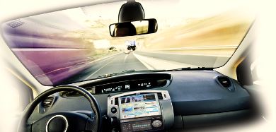
People spend a significant amount of time in their cars, whether commuting to work, going to the mall with the kids, or taking a road trip with loved ones. The car has evolved into an extension of our lives outside the home that blend driving fun with full featured electronics that give people a consumer device interface. In-car electronics have also moved beyond entertainment and fancy HMI (human-machine interface) displays to include intelligent safety monitoring and occupant protection systems. The automotive OEMs that build compelling consumer centric HMI / entertainment IVI (in-vehicle infotainment) and advanced safety features will be the ones driving higher automobile sales, and the best sellers will be the ones that create the most immersive in-car living room experience in a safe environment where the vehicle is “aware” of its surroundings. New GPU technologies enable automotive OEMs to realize both types of technologies with 3D graphics for visual eye candy and GPGPU (General Purpose Graphics Processing Unit) using OpenCL for safety applications. Upcoming vehicles shipped will have a predefined set of functions available on the HMI or IVI, but the car owner will be able to install different apps to customize the car interface. GENIVI (www.genivi.org) is an example of an open platform, industry consortium taking IVI to the next level.
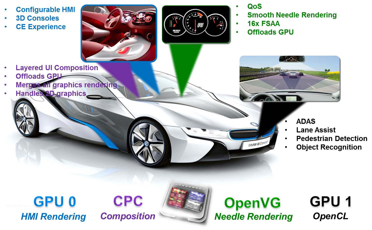
3D Graphics
3D graphics have been heavily used in the mobile market with the rapid expansion of Android and iOS. Each successive release of a mobile operating system or hardware technology pushes the visual envelope in terms of UI, 3D game play and captivating visual content. Since consumers are familiar with the look and feel of their existing mobile devices, the automotive market has taken note of this and started looking at in-vehicle platforms that display information in a similar manner. The first generation automobiles with embedded GPUs had basic graphics functionality which was limited in performance and capabilities since graphics was not an important requirement during the time that pre-dated the first iPhone shipments. Once the iPhone took off, adoption of GPU IP into system-on-chips (SOC) really took off and brought graphics into the spotlight where it could make-or-break a product. With this new paradigm shift, graphics proliferated into many important markets including the automotive industry where some SOC vendor designs are awarded based on the GPU inside.
Leveraging the mass market use of 3D graphics in mobile devices and building on the existing ecosystem around 3D graphics, dynamic and fancy UIs, and apps, automotive OEMs are using these building blocks to transform themselves from car makers to a new breed of consumer-focused automotive manufacturers that have the HW (car) and SW (apps, app store) to turn the driving experience upside down. One step to create this transition to their new business model is to bring the familiar graphical interfaces and user experiences found on tablets and TVs and transform the car into an entertainment hub powered through the IVI system and driver HMIs to add eye candy to console data displays. These displays need to scale to higher resolutions with higher DPI on HD screens that are crisp, clear, vivid, and responsive. The migration towards a visual-centric automobile console shows the importance of the GPU and how it has changed from a nice-to-have feature to a must-have requirement that sways technology decisions in the automotive ecosystem. The technology is available to put the pieces together in terms of hardware, software, middleware, and operating systems – it just comes down to putting the pieces together to make the final product and bringing the next generation graphics-centric solutions to a dealer near you, that goes beyond what is available today.
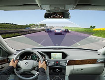
Safety Features
Safety is another major feature that influences purchase decisions. The term ADAS or Advanced Driver Assistance Systems describes the latest electronic technologies found in vehicles that focus on increasing safety for occupants, pedestrians, and surrounding vehicles. Features included in ADAS that monitor, predict, and try to prevent accidents include active safety monitoring, collision avoidance systems (CAS), object/pedestrian recognition, land departure warning, adaptive cruise control, and more. Current solutions use a combination of DSPs, CPUs, and in some cases FPGA with built-in computational units to perform safety monitoring. These solutions use hand written code for specific products, making them harder to port to new platforms or when changing components like DSPs or CPUs. With the GPU you can overcome these limitations by writing algorithms in OpenCL (described in more detail later) with some GPU based OpenCV libraries, and the code can be re-used across various platforms since it is cross platform compatible. In the near future, the compiler will be able to partition code to be executed on the most efficient compute element (GPU, CPU, DSP) in a platform to give the best overall performance. Parallel data will go to the GPU and serial data can go to the DSP or CPU.
Some automakers are looking at harnessing the massively parallel processing power of GPUs to reduce parallel algorithm execution times and speed-up real-time response in ADAS. Since the GPU is inherently fast at image and pixel processing, incoming pixel data from camera sensors and other sensors that are parallel in nature can be sent through the GPU to be processed. In addition GPGPU APIs like OpenCL can help process parallel data streams (sensor fusion) from cameras, GPS/WiFi positioning data, accelerometers, radar, and LIDAR to guide vehicles safely. Current solutions focus on computer vision (CV) as a first step, but moving forward data from other sensors can be sent to the GPU to offload other computational resources in a system. Autonomous cars like Google’s driverless car and those in DARPA competitions have already demonstrated what the future of ADAS will evolve into.
Entertainment and safety can be met with the latest semiconductor technologies like those found in the Freescale i.MX 6 automotive grade applications processors to enhance 3D/2D/VG graphics (HMI rendering, games, and user interface composition) and OpenCL (ADAS, computer vision, and gesture). So far the i.MX 6 is the only product that targets automotive with advanced graphics like OpenGL ES 3.0 and GPU compute with OpenCL 1.1.
Source: Mercedes Benz
The Evolution of GPUs from Graphics to General Purpose Computation Cores (GPGPU)
The GPU was originally designed for 3D graphics applications and image rendering during the rasterization process. Over time the computational resources of modern graphics processing units became suitable for certain general parallel computations due to the massively parallel processing capabilities native to GPU architecture. Graphics is one of the best cases of parallel processing where the GPU needs to execute on billions of pixels or hundreds of millions of triangle vertices in parallel.
GPU architectures process independent vertices, primitives and fragments in great numbers using a large number of graphics shaders, which are also known as arithmetic logic units (ALUs) in the CPU world. Each primitive is processed the same way, using the same program or kernel. Many computational problems like image processing, analytics, mathematical calculations and others map well to this single-instruction-multiple-data (SIMD) architecture. The calculation speed-up shown and proven on SIMD processors was quickly recognized by researchers and developers and another area of high performance computing built on the vast processing power of GPUs was born. Today and in the near future, the fastest supercomputers and processing units use or will use GPU technology for the highest compute performance, calculation density, time savings, and overall system speed-up. The GPU has morphed from a graphics processor into a general purpose co-processor that sits alongside the CPU in today’s platforms.
The Penalties That Come With Less Than Optimal Graphical Processing
When selecting a GPU, there are certain requirements that need to be met when it comes to performance, power, and capabilities. Performance not only includes graphics benchmark results and 3D games, but also testing different applications that mirror real world use cases so the applications processor and GPU give the best overall user experience. As screen resolutions increase in both mobile devices and in-vehicle screens, the pixel count and triangle count (3D complexity) go up, leading to higher demand on the GPU as more objects need to be rendered onscreen. An underpowered GPU will lead to low performance (dropped frames, low FPS, image artifacts, incorrect rendering) and pretty much a non-usable device as evidenced by some of the first generation tablets that shipped but never used extensively. To get to the latest consumer electronics product levels, the GPUs in cars need to be upgraded from OpenGL ES 1.1 graphics to ES 2.0 and ES 3.0 capable cores with added shader performance to create eye catching visuals. i.MX 6 was one of the first SoCs where graphics was specifically defined at the product planning stages as Freescale had a vision of the car as a node in the internet of things (IOT) and graphics as the interface that couples man and machine. Content for cars (streamed media, social, games, apps) is also increasing as they become digitally connected with the rest of the consumer ecosystem. i.MX 6 is currently the only automotive SoC to support the latest APIs including OpenGL ES 3.0 and OpenCL 1.1. Other SoCs from Texas Instruments, Renesas, and FPGA based solutions have graphics capabilities, but rely on other solutions for OpenCL
The evolution of in-vehicle graphics went from an afterthought to a must have feature, migrating from simple onscreen text (that either used the CPU or simple 2D engine), to 2D graphics and then basic 3D. Today, there is another transition to advanced GPU rendering as seen on consumer devices that show detailed 3D models of your car in the console to highlight parts of the car in an easier to see format, 3D maps with street and building details, customizable/configurable HMI consoles similar to personalizing our Android smartphone, and much more. The initial solutions were underpowered but over time consumer expectations have grown to match their mobile devices going from a UI that was either scaled down or limited (ex. less icons, less menu layers, and basic 3D graphics) by specific hardware, to products that blur the line between consumer and auto.
According to Richard Robinson, principal analyst for automotive infotainment at iSuppli, “Infotainment hardware has undergone a rapid evolution during the last 13 years, moving from the traditional approach of dedicated hardware blocks, to the advent of bus-connected distributed architecture systems in the 2000 time frame, to the highly-integrated navigation-centric systems of 2006, to the new user-defined systems of today.”1
“The traditional boundaries between home, mobile and automotive infotainment systems are quickly going away. Consumers are now expecting the same features and equal access to their data across all these platforms,” said Jim Trent, VP and GM at NEC Electronics America2.
An Overview of OpenCL and Its Benefits.
OpenCL (Open Computing Language) is an open industry standard application programming interface (API) used to program multiple devices including GPUs, CPUs, as well as other devices organized as part of a single computational platform. The standard targets a wide range of devices from consumer electronics (smartphone, tablets, TVs) to embedded applications like automotive ADAS and computer vision (CV). Applications that already take advantage of the OpenCL performance speedup include medical imaging, video/image processing, high performance computing (HPC), robotics, surveillance, “Big Data” analytics, augmented reality, and gesture (motion, NUI). We will focus on the GPU aspect of OpenCL below.
The evolution of GPU computing has gone through a few major milestones. Pre-OpenCL, a program would be specifically written for and executed on a target device. This limited the features, performance, and calculation throughput to the device characteristics and there was not much flexibility beyond the hardware’s capabilities. The next step forward was the introduction of OpenCL where a hardware abstraction layer is created that separates the application from what is “under-the-hood” for ease of use and cross-platform portability. The abstraction layer queries all computational resources in a platform and uses them in the best way as a single cohesive unit to leverage as much computing horsepower as possible. Moving forward as we progress from OpenCL 1.1/1.2 to 2.0, advanced API features will be added along with making the solution even easier for general purpose programming.
At a high level, OpenCL provides both a programming language and a framework to enable parallel programming. The programming language is based on ISO C99 with math accuracy based on the IEEE 754 standard. OpenCL also includes libraries and a runtime system to assist and support software development. A developer can write general purpose OpenCL programs that executes directly on a GPU without needing to know 3D graphics or 3D APIs like OpenGL or DirectX. OpenCL also provides a low-level hardware abstraction layer as well as a framework that exposes many details of the underlying hardware layer allowing the programmer to take full advantage of it.
OpenCL uses the parallel execution SIMD (single instruction, multiple data) engines to enhance data computation density by performing massively parallel data processing on multiple data items, across multiple compute engines. Each compute unit has its own ALUs, including pipelined floating point (FP), integer (INT) units, and a special function unit (SFU) that can perform computations as well as transcendental operations. The parallel computations and associated series of operations is called a kernel, and the Vivante cores can execute millions of parallel kernels at any given time.
A Deeper Discussion of Graphics and OpenCL Benefits using Freescale’s i.MX 6 As An Example
Freescale uses GPU technology from a leading GPU IP provider based in Sunnyvale, California called Vivante to provide the 3D graphics, OpenVG, and OpenCL compute capability in their automotive grade i.MX 6 product line3. The i.MX6 applications processor is the industry’s first scalable, multicore ARM Cortex-A9 product line that spans single, dual, and quad core CPU architectures that are pin and software compatible. Integrated into the i.MX 6 is the GC2000 3D and OpenCL GPU, GC355 for fast hardware OpenVG acceleration, and the GC320 composition processing core (CPC) to compose screen content which the user sees. The applications processor also integrates the image processing unit (IPU) that accepts multiple camera input streams into the i.MX 6 for processing (ex. 360 degree view, rear view camera, and blind-spot detection).
The 3D graphics core provides 200 million triangles per second rendering horsepower which rivals performance of some of the latest tablets and smartphones, enabling the i.MX 6 to render ultra-realistic graphics and connect to app stores to play the latest games and display 3D UIs4. With this built-in capability and performance, ecosystem partners like QNX, Green Hills, Adeneo, Mentor Graphics, Rightware, Electrobit, and others are optimizing their operating systems, middleware, and applications to efficiently run the full feature set of the i.MX 6 GPU. The Freescale development platforms also have BSPs (board support packages) for Android and Linux to aid in the development of platforms in similar markets.
The OpenCL support currently focuses on accelerating Embedded (Computer) Vision applications that rely on camera inputs for ADAS. Some example applications where OEMs are analyzing GPU OpenCL performance are:
- Feature Extraction – this is vital to many vision algorithms since image “interest points” and descriptors need to be created so the GPU knows what to process. SURF (Speeded Up Robust Features) and SIFT are examples of algorithms that can be parallelized effectively on the GPU. Object recognition and sign recognition are forms of this application.
- Image filtering with different kernel sizes to enhance images.
- Integral image for image acquisition can be spread across multiple i.MX 6 GPU shaders to cut down calculation time and parallelize execution.
- Resampling – the GPU can use texture sampling to perform bilinear or bicubic filtering.
- Point Cloud Processing – includes feature extraction to create 3D images to detect shapes and segment objects in a cluttered image. Uses could include adding augmented reality to street view maps.
- Line detection – uses Hough Transform to detect lines in the input image (creates edge maps) followed by Sobel or Canny algorithms to further enhance edge detection. This can be used for lane detection
- Pedestrian Detection – uses Histogram of Oriented Gradients (HOGS) to detect a person and automatically brake the car if the driver does not react in time.
- Face recognition – goes through face landmark localization (exl Haar feature classifiers), face feature extraction, and face feature classification. Another use could be eye recognition to detect drowsiness and keep the vehicle within its lane.
- Hand gesture recognition – separates hand from background (ex. color space conversion to the HSV color space) and then performs structural analysis on the hand to process motion.
- Camera image de-warping – GPU performs matrix multiplications to map wide-angle camera inputs onto a flat screen so images are corrected. OEMs can use different camera vendors and to de-warp images they would only need to use different camera coefficients making the GPU easy to program.
- Blind-spot detection – cameras can be used for blind spot detection using OpenCL to process stereo images. In this case, two cameras are needed per blind spot to detect depth so the GPU knows how far/close the other car is.
There applications listed above are examples of where OEMs are looking at using OpenCL on the GPU to speed up ADAS. There are many exciting
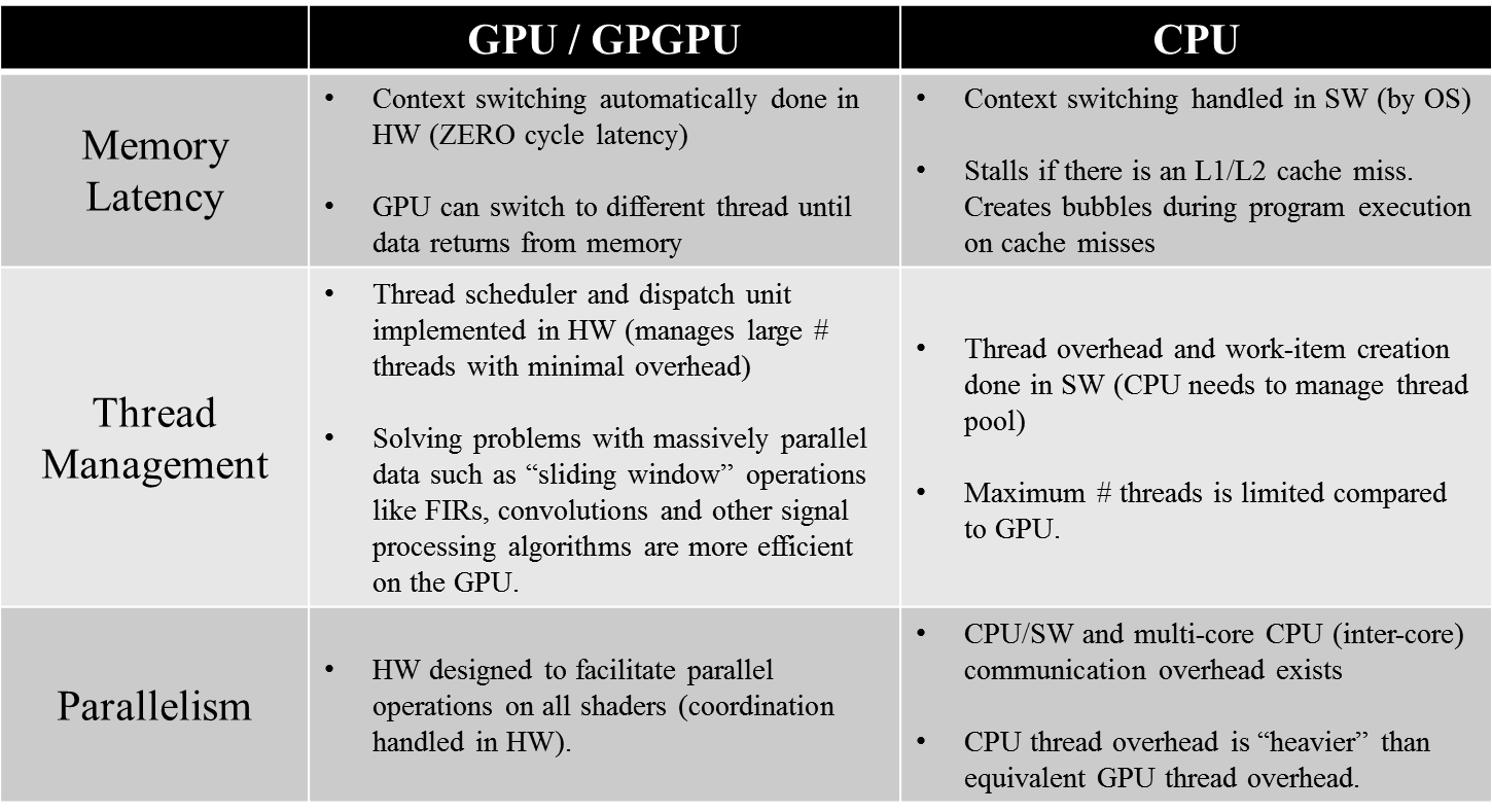
Background information: GPU vs. CPU for processing OpenCL
The best approach is to use a hybrid/heterogeneous platform (ex. HSA) to accelerate applications. CPU for task parallelism and serial computations & GPU for data parallel processing.
Notes:
- http://www.isuppli.com/Automotive-Infotainment-and-Telematics/News/Pages/Automotive-Infotainment-Hardware-Enters-Fourth-Generation-Stage.aspx
- http://www.genivi.org/sites/default/files/press-releases/english/2009_11_10_GENIVI_Expands.pdf
- http://www.eetimes.com/electronics-news/4375956/Freescale-Vivante-Rightware-automotive-display
- http://www.cnx-software.com/2012/01/19/freescale-i-mx6-automotive-aerospace-infotainment-applications/
HSA Releases Ver. 0.95 of PRM Specification
By Benson Tao (Vivante Corporation)
![]()
Background
The Heterogeneous System Architecture (HSA) Foundation is a not-for-profit consortium that brings together some of the best minds (and companies) across the mobile, PC, consumer, HPC, Compute/Vision industries, along with leading academic institutions and anyone that wants to join in on the fun. The goal of HSA is to create a single architecture specification and standard programming interface (API) that developers can easily adopt to optimize distributed workloads across the GPU, CPU, DSP, and any other compute fabric element on the platform. From a high level view, the platform or system (with all the different components) can be viewed as one large, unified processor that executes a given workload. The main goal is to get the biggest bang for the buck or operational efficiency that includes the highest computational throughput (performance) at the lowest power and thermal envelope. Industry participants in HSA include SoC vendors, IP providers, OEMs, OSVs, and a full range of ISVs and application developers that want to make the best use of platform capabilities.
Vivante Contributes to Platform Innovation
Vivante joined HSA Foundation with the intention of pushing forward a defined specification that advances GPU Compute technologies in mobile, embedded, and consumer platforms. Many of our new and existing customers look to us for guidance on ways to improve their existing platforms and problems they are “stuck” on. Improvements can be as minor as performance gains, reduced BOM (or silicon) costs, and power savings, to re-architecting their designs (through GPU programmability) to fit new use cases and applications so they can extend product lifecycles without incurring major financial costs to replace/upgrade the existing infrastructure. These are some of the ways Vivante looks at defining solutions and future-proofing GPU/GPGPU IP cores to help its customers.
Vivante has multiple products targeting hybrid platforms from mass market cores that have the smallest silicon footprint with OpenGL ES 3.0 and OpenCL 1.1/RS-FS, to mid range and high performance multi-cluster configurable cores. The GPUs work directly with the CPU through a unified memory system, ACE-Lite™ cache coherency, or a native stream interface that connects directly to various compute fabrics. The Vivante HSA design, like the OpenGL ES graphics stack, supports a unified software and hardware package that provides a single architecture spanning multiple operating systems, platforms, and GPU cores. Vivante HSA software will also be backwards compatibility with all existing compute-enabled products and built around HSA APIs and tools that complement our current OpenCL™ and Google Renderscript™/Filterscript support. By simplifying the lives of application developers targeting heterogeneous architectures, programmers can create breakthrough use cases that take advantage of the new paradigm shift to hybrid computing. Real world applications that are already being accelerated by Vivante cores include computer vision, image processing, augmented reality, sensor fusion, and motion processing, with some examples being in the automotive ADAS sector (Advanced Driver Assistance Systems).
HSA Releases Ver. O.95 of the Highly Anticipated Programmers Reference Manual (PRM)
The fruits of hard labor of many technical discussions and architecture meetings over the last year since the consortium’s founding in June 2012 has finally come full circle with the release of version 0.95 of the PRM. This manual is a major milestone and lays the foundation for HSA to successfully move forward as it continues defining the platform of the future. The PRM also gives developers an early start as ecosystem partners create amazing applications, tools, libraries, and middleware programs that work best on HSA certified products.
Some features highlighted in the specification include:
1) Shared Coherent (Virtual) Memory Models
2) Atomics
3) User Mode and GPU Queuing
4) Zero Copy
5) Low Latency Dispatch
The specification also includes HSAIL (HSA Intermediate Language), which abstracts away from the native instruction set of the hardware and can be compiled automatically, in real-time, to the native ISA of the underlying hardware without any developer involvement. The same OpenCL and Renderscript/Filterscript programs can be abstracted and run on HSA platforms also.
Link to HSA Foundation website: http://hsafoundation.com/
Link to HSA Foundation press release: http://hsafoundation.com/hsa-foundation-announces-first-specification/
