

GC Nano User Interface (UI) Acceleration

Background and Overview
Crisp, clear, and responsive user interface HMI (human machine interface) has become equally important to the user experience as the content or the device form factor. A beautifully crafted smartphone that uses a combination of brushed titanium and smudge-proof glass may look great in the hand, but the user will quickly opt for another product if the user interface stutters or the screen is hard to read because of aliased and inconsistent fonts. The same scenario also applies to HMI in wearables and IoT devices, which is the focus of this white paper.
The goal of a well-designed wearable/IoT HMI is to make reading or glancing at the screen intuitive and natural, yet engaging. In other words, it is about a consistent, seamless interaction between user and device. Since device screens are smaller, information needs to be displayed in a simplified, uncluttered way with only relevant data (text, images, icons, video, etc.) rendered and composed onscreen. Smaller device screens do not directly translate into a device with less processing capabilities. The opposite can be true since upcoming devices need to perform real time processing (UI display composition, communications, sensor processing, analytics, etc.) as part of a single or network of IoT nodes. Some wearables/IoTs are taking technologies found in low/mid-range smartphone application processors and customizing parts of the IP specifically for wearables. One important IP that device OEMs need is the graphics processing unit (GPU) to accelerate HMI screen composition at ultra-low power.
In addition, a couple hot new trends in these emerging markets is personalized screen UI or a unified UI that spans all devices from cars and 4K TVs, to smartphones, wearables and embedded IoT screens to give users a consistent, ubiquitous screen experience across a given operating system (OS) platform, regardless of the underlying hardware (i.e. SoC/MCU). This will enable a cross vendor solution where vendor A’s smartwatch will work correctly with vendor B’s TV and vendor C’s smartphone. Google and Microsoft have recently announced support for these features in their Android Material Design and Windows 9 releases, respectively. Support for this requires an OpenGL ES 2.0 capable GPU at the minimum, with optional/advanced features using OpenGL ES 3.x. Google also has their light weight wearables OS called Android Wear that requires a GPU to give the UI a similar look-and-feel as their standard smartphone/tablet/TV Android OS.

Figure 1: Evolving Wearable and IoT Devices Requiring GPUs
Vivante GPU Product Overview
The underlying technology that accelerates HMI user experience is the graphics processing unit (GPU). GPUs natively do screen/UI composition including multi-layer blending from multiple sources (ISP/Camera, Video, etc.), image filtering, font rendering/acceleration, 3D effects (transition, perspective view, etc.) and lots more. Vivante has a complete top-to-bottom product line of GPU technologies that include the GC Vega and GC Nano Series:
- GC Vega Series targets SoCs that need the latest and greatest GPU hardware and features like OpenGL ES 3.1, Full Android Extension Pack (AEP) Support including hardware tessellation / geometry shaders (TS/GS), DirectX 12, close to the metal GPU programming, hybrid ray tracing, zero driver overhead, sensor fusion, and GPU-Compute for vision processing using OpenVX, OpenCV or OpenCL, bundled in the most aggressive PPA and feature-complete design. Target markets range from high end wearables and low/mid-range mobile devices up to 4K TVs and GPUs for server virtualization.
- GC Nano Series falls on the other side of the spectrum and targets devices that are making a revolutionary push into consumer products like wearables and IoT (smart homes / appliances, information gadgets, etc.) with GPU rendered HMI / UI. This core is specifically designed to work in resource constrained environments where CPU, memory (both on-chip and DDR), battery, and bandwidth are very limited. GC Nano is also optimized to work with MCU platforms for smaller form factors that require UI composition acceleration at 30/60+ FPS.

Figure 2: Vivante GPU Product Line and Target Markets
GC Nano Overview
GC Nano Series consists of the following products starting with the GC Nano Lite (entry), GC Nano (mainstream) and GC Nano Ultra (mid/high).

Figure 3: GC Nano Product Line
GC Nano Series benefits include:
- Silicon Area and Power Optimized: Tiny silicon footprint that maximizes performance-per-area for silicon constrained SoCs means vendors can add enhanced graphics functionality to their designs without exceeding silicon/power budgets and still maintain responsive and smooth UI performance. GC Nano maximizes battery life with ultra-low power consumption and thermals with minimal dynamic power and near zero leakage power.
- Smart Composition: Vivante’s Immediate Mode Rendering (IMR) architecture reduces composition bandwidth, latency, overhead and power by intelligently composing and updating only screen regions that change. Composition works either with GC Nano composing all screen layers (graphics, background, images, videos, text, etc.) or through a tightly coupled design where the GC Nano and display controller/processor (3rd party or Vivante DC core) work in tandem for UI composition. Data can also be compressed / decompressed through Vivante’s DEC compression IP core to further reduce bandwidth.
- Wearables and IoT Ready: Ultra-lightweight vector graphics (GC Nano Lite) and OpenGL ES 2.0 (GC Nano, GC Nano Ultra) drivers, SDK and tools to easily transition wearables and IoT screens to consumer level graphical interfaces. The GCcNano package also includes tutorials, sample code, and documentation to help developers optimize or port their code.
- Designed for MCU/MPU Platforms: Efficient design to offload and significantly reduce system resources including complete UI / composition and display controller integration, minimal CPU overhead, DDR-less and flash memory only configurations, bandwidth modulation, close-to-the-metal GPU drivers, and wearables / IoT-specific GPU features to shrink silicon size. The tiny software code size puts less constraints on memory size, speeds up GPU initialization/boot-up times and allows instant-on UI composition for screens that need to display information at the push of a button.
- Ecosystem and Software Support: Developers can take advantage of the lightweight NanoUI or OpenGL ES API to further enhance or customize their solutions. Large industry support on existing Vivante products include the GC Nano / GC Nano Ultra product line on Android, Android Wear and embedded UI solutions from key partners covering tools for font, artwork and Qt development environments.
- Compute Ready: As the number of wearable / IoT (processing) nodes grows by several tens of billions of units in the next few years, bandwidth on data networks could be an issue with an always-on, always-connected, always-processing node. GC Nano helps with this by performing ultra-low power processing (GFLOP / GINT ops) at the node and only transmits useful compressed data as needed. Examples include sensor fusion calculations and image/video bandwidth reduction.
Vivante’s software driver stack, SDK and toolkit will support its NanoUI API that brings close-to-the-metal GPU acceleration for no-OS / no-DDR options on GC Nano Lite and the OpenGL ES 2.0 API (optional 3.x) for more advanced solutions that include proprietary or high-level operating systems like embedded Linux, Tizen™, Android™, Android™ Wear and other RTOS that require OpenGL ES 2.0+ in the smallest memory footprint. These various OS / non-OS platforms will form the base of next generation wearables and IoT that bring personalized, unique and optimized experiences to each person. The GC Nano drivers include aggressive power savings, intelligent composition and rendering, and bandwidth modulation that allow OEMs and developers to build rich visual experiences on wearables and IoT using an ultralight UI / composition or 3D graphics driver.
Many of the GC Nano innovations create a complete “visual” wearables MCU/SoC platform that optimizes PPA and software efficiency to improve overall device performance and BOM cost, with the most compact UI graphics hardware and software footprint that does not diminish or restrict the onscreen user experience. These new GPUs are making their way into some exciting products that will appear all around you as wearables and IoT get integrated into our lives.

Figure 4: GC Nano Series Features and Specifications

Figure 5: Example GC Nano Series SoC/MCU Implementation
Trends and Importance of 3D User Interface Rendering
In the UI sample in Figure 6 of a smart home device, next generation products will take some of the well thought out UI design elements from smartphones, tablets and TVs and incorporate them into IoT devices (and wearables) to keep a consistent interface between products. The similar UI look-and-feel will reduce usage learning curve and accelerate device adoption. As a side note, since different devices have different levels of processing/performance capabilities, a minimum level will be used for smaller screens (baseline performance) with additional features/higher performance added as device capabilities move up into a higher tier segmented by the OS vendor.

Figure 6: Sample HMI user interface on a smart home device
A few examples of updated UIs include the following:
- Animated icons – easily shows the user which menu item is selected or where the input cursor is pointed to so the user does not need to spend time searching for cursor position onscreen. Icons can rotate, wiggle, pop out, flash, etc. before being selected.
- Live animations – dynamic content can turn a simple background (wall paper) into a dynamic moving scene that can add a personal touch to your device. Background images and designs can also be personalized to match décor, lighting, theme and mood. Some white good appliance makers are testing these concept designs, hoping to put one (or two) inside your kitchen in the near future.
- 3D effects – text, icons and images that go beyond simple shadows where feature of the GPU can render using powerful shader instructions to give 3-dimensional character to parts of the UI (ex. carousel, parallax, depth blur, widget/icon rendering to 3D/2D shapes, procedural/template animations for icon movements, physical simulations for particle systems, perspective view, etc.). These effects can be implemented using the GC Nano’s ultra-low power OpenGL ES 2.0/3.x pipeline.
GC Nano’s architecture excels at HMI UI composition by bringing out 3D UI effects, bandwidth reduction and reduced latency, which will be discussed below.
GC Nano Bandwidth Calculation
In this section we will step through examples of various user interface scenarios and calculate system bandwidth for both 30 and 60 FPS UI HMI rendering through the GC Nano GPU. All calculation assumptions are stated in section 5.2.
Methods of Composition
There are also two options for screen display composition that we will evaluate – first, where the GPU does the entire screen composition of all layers (or surfaces) including video and the display controller simply outputs the already composited HMI UI onscreen, and second, where the display controller takes composited layers from both GPU and video decoder (VPU) and does the final UI composition blend and merge before displaying. The top level diagrams below do not show DDR memory transactions, but they will be shown in section 5.2 when describing the UI steps.

Figure 7: GC Nano Full Composition: All UI layers are processed by GC Nano before sending the final output frame to the display controller

Figure 8: Display Controller Composition: Final output frame is composited by the display controller using input layers from GC Nano and the video processor
UI Bandwidth Calculations
Calculation assumptions:
- GC Nano UI processing is in ARGB8 (32-bits per pixel) format. When GC Nano performs full composition, the GPU automatically converts 16-bit YUV video format into 32-bit ARGB.
- Video frame is in YUV422 (16-bits per pixel) and has the same resolution as the screen size (GC Nano treats incoming video as video textures)
- Final composited frame is in ARGB8 format (32-bits per pixel)
- Reading video has a request burst size of 32-bytes
- GC Nano UI request burst size is 64-bytes
- Write sizes for writing out the UI rendering and final frame is 64-bytes
- For these cases we assume 32-bit UI rendering. If the display format is 16-bits (applicable to smaller screens) then the bandwidth calculations listed below will be much lower.
- Bandwidth calculation examples will be given for WVGA (800×480) and 720p (1280×720)
- The amount of UI pixels per frame that need to be refreshed/updated (in our example) will include the following percentages:
- 15% (standard UI)
- 25%
- 50% (worst case UI)
GC Nano Full UI Composition
The following images describe the flow of data to/from DDR memory using GC Nano to perform the entire UI composition. Some major benefits of using this method include using the GPU to perform some pre-post processing on images or videos, filtering, adding standard 3D effects to images/videos (video carousel, warping/dewarping, etc.) and augmented reality where GC Nano overlays rendered 3D content on top of a video stream. This method is the most flexible since the GC Nano can be programmed to perform image/UI related tasks.


Figure 9: GC Nano Full Composition memory access and UI rendering steps (steps 1 – 4)
Bandwidth calculation is as follows:

Notes:
- Total screen pixels = resolution WxH
- UI pixels updated per frame = [Total screen pixels] * [UI% updated per frame]
- Total UI pixels updated per frame in bytes = [UI pixels updated per frame] * [4 Bytes]; 4 Bytes since the UI format is 32bpp ARGB8888
- Assumes video is in the background (worst case). Total composition Bandwidth (Bytes) = Video part [(a – c) * (2 Bytes for 16-bit YUV)] + UI part [c * 4 Bytes for ARGB8] + [a * 4 Bytes]
- Total bandwidth per frame (MB) = [(c+d)/106]
- Total bandwidth = [e*30] for 30 FPS and [e*60] for 60 FPS
Display Controller UI Composition
This section describes the flow of data to/from DDR memory using the display controller to do the final merging/composition of layers from the GC Nano and video processor. This method partially reduces bandwidth consumption since the GPU does not need to read in the video surface since it does not perform final frame composition. The GPU only works on composing the UI part of the frame minus any additional layers from other IP blocks inside the SoC/MCU. A benefit from this method is lower overall system bandwidth, but at the cost of less flexibility in the UI. If the video (or image) stream only needs be merged with the rest of the UI then this is a good solution. If the incoming video (or image) stream needs to be processed in any way – adding 3D effects, filtering, augmented reality, etc. – then this method has limitations and it is better to use the GPU for full frame UI composition.

Figure 10: Display controller performing final frame composition from two incoming layers from GC Nano and the video processor (VPU)
The display controller has a DMA engine that can read data from system memory directly. Data formats supported are flexible and include various ARGB, RGB, YUV 444/422/420, and their swizzle formats.
Bandwidth calculation for UI composition only is straightforward and is only based on the screen resolution size, as follows:

Notes:
- Total screen pixels = resolution WxH
- Total UI pixels per frame = [Total screen pixels] * 4 Bytes; 32-bit ARGB8 format
- Total bandwidth per frame (MB) = [b/106]; since GC Nano needs to perform full screen UI minus additional layers from other sources
- Total bandwidth = [c*30] for 30 FPS and [c*60] for 60 FPS
Summary of Bandwidth Calculations
The table below summarizes the calculations above:

Adding Vivante’s DEC compression technology will also reduce bandwidth by about 2x – 3x from the numbers above.
GC Nano Architecture Advantage for UIs
There are two main architectures for GPU rendering, tile based rendering (TBR) and immediate mode rendering (IMR). TBR breaks a screen image into tiles and renders once all the relevant information is available for a full frame. In IMR graphics commands are issued directly to the GPU and executed immediately. Techniques inside Vivante’s architecture allows culling of hidden or unseen parts of the frame so execution, bandwidth, power, etc. is not wasted on rendering parts of the scene that will eventually be removed. Vivante’s IMR also has significant advantages when rendering photorealistic 3D images for the latest AAA rated games that take advantage of full hardware acceleration for fine geometries and PC level graphics quality, including support of advanced geometry/tessellation (GS/TS) shaders in its high end GC Vega cores (DirectX 11.x, OpenGL ES 3.1 and Android Extension Pack – AEP). Note: some of the more advanced features like GS/TS are not applicable to the GC Nano Series.
Tile Based Rendering (TBR) Architecture for UIs
The following images explain the process TBR architectures use for rendering UIs.
Breaking a scene into tiles…

But…before rendering a frame, all UI surfaces need to go through a pre-tile pass before proceeding…

Combining the pre-processing step and tiling step give us the following…

If the UI is dynamic then parts of the frame need to be re-processed…

Here are the “dirty” blocks inside the UI

TBR UI Rendering Summary
From the steps shown above, TBR based GPUs have additional overhead that increases UI rendering latency since the pre-processed UI triangles need to be stored in memory first and then read back when used. This affects overall frame rate. TBR GPUs also require large amounts of on-chip L2$ memory to store the entire frame (tile) database, but as UI complexity grows, either the on-chip L2$ cache size (die area) has to grow in conjunction or the TBR core has to continuously overflow to DDR memory which increases their latency, bandwidth and power.
TBRs have mechanisms to identify and track which parts of the UI (tiles) and which surfaces have changed to minimize pre-processing, but for newer UIs that have many moving parts; this continues to be a limitation. In addition, as screen sizes/resolutions and content complexity increases, this latency becomes even more apparent especially on Google, Microsoft, and other operating system platforms that will use unified UIs across all screens.
Immediate Mode Rendering (IMR) Architecture for UIs
The most advanced GPUs use IMR technology, which is object-based rendering found in PC (desktop/notebook) graphics cards all the way to Vivante’s GC Series product lines. IMR allows the GPU to render photorealistic images and draw the latest complex, dynamic and interactive content onscreen. In this architecture, graphics API calls are sent directly to the GPU and object rendering happens as soon as commands and data are received. This significantly speeds up 3D rendering performance.
In the case of UIs, the pre-pass processing is not required and this eliminates the TBR-related latency seen in section 6.1. In addition, there are many intelligent mechanisms that perform transaction elimination so hidden (unseen) parts of the frame are not even sent through the GPU pipeline, or if the hidden portions are already in-flight (ex. change in UI surface), those can be discarded immediately so the pipeline can continue executing useful work.
Composition processing is performed in the shaders for flexibility and the Vivante GPU can automatically add a rectangle primitive that takes the whole screen into account to achieve 100% efficiency (versus 50% efficiency using two triangles). Memory bandwidth is equivalent to TBR architectures for simple UIs and 3D frames, but for more advanced UIs and 3D scenes, TBR designs need to access external memory much more than IMR since TBRs cannot hold large amounts of complex scene data in their on-chip caches.
The following images explain the process Vivante’s IMR architecture uses for rendering dynamic UIs. The process is significantly simpler compared to TBRs, and dynamic changes in UI or graphics are straightforward.
IMR Object Based UI Rendering

Additional UI Content are Considered New Objects

IMR GPUs are Ideal for Dynamic and Next Gen UIs

IMR UI Rendering Summary
For dynamic 3D UIs, complex 3D graphics, mapping applications, etc., IMRs are more efficient in terms of latency, bandwidth and power. Memory consumption and memory I/O is another area where IMR has its advantages – for upcoming dynamic real time 3D UIs, IMR is the best choice and for standard UIs, IMRs and TBRs are equivalent but IMRs give the SoC/MCU flexibility and future-proofing. Note: historically, TBRs were better for simpler UIs and simple 3D games (low triangle/polygon count, low complexity) since TBRs could keep the full frame tile database on chip (L2$ cache), but advances in UI technologies brought about by leading smartphones, tablets and TVs have tipped things in favor of IMR technology.
Summary
GC Nano provides flexibility and advanced graphics and UI composition capabilities to SoCs/MCUs targeting IoT and wearables. With demand for high quality UIs that mirror other consumer devices from mobile to home entertainment and cars, a consistent, configurable interface is possible across all screens as the trend towards a unified platform is mandated by Google, Microsoft and others. GC Nano is also architected for OEMs and developers to take advantage of IMR technologies to create clean, amazing UIs that help product differentiation. The tiny core packs enough horsepower to take on the most demanding UIs at 60+ FPS in the smallest die area and power/thermal consumption. The GC Nano also reduces system bandwidth, latency, memory footprint and system/CPU overhead so resource constrained wearables and IoT SoCs/MCUs can use GPUs for next generation designs.

GCNano GPUs – Supercharging your Wearables and IoT
Vivante recently announced the GCNano GPU Series, the latest product line that complements its shipping Vega GC7000 Series to complete the world’s first full line-up of top to bottom GPU offerings, from the smallest wearables and IoT devices, to ultra HD 4K / 8K TVs, smartphones and tablets. GC7000 targets SoCs that need the latest and greatest GPU hardware and features like OpenGL ES 3.1, Full Android Extension Pack Support, DirectX 12, tessellation / geometry shaders, ray tracing, zero driver overhead and GPGPU for vision / image / physics processing, with the most aggressive PPA and feature-complete design. GCNano falls on the other side of the spectrum without sacrificing features or performance, and targets devices that are making a revolutionary (visual user interfaces / UI, network connected, intelligence) push into consumer products like wearables and IoT (smart homes / appliances, information gadgets, etc.). Many of these new products will be powered by microcontroller (MCU) and microprocessor (MPU) systems that will complement the general purpose applications processors (AP) found in mobile and home entertainment products. (I’ll use the term MCU to collectively reference MCUs and MPUs).
About MCUs
MCUs are task specific “embedded” processing devices that are found in the billions inside everything from the washing machine control / interface and thermostats with displays, to remote controls, network printers with displays, smart meters, and other devices in the home, car, infrastructure or on the body. Most of them are invisible to us, but behind the scene they keep our world moving. Traditional MCUs only supported basic visual interfaces since their focus was to display relevant information and keep things simple. Over the last several years the industry took a sharp turn and evolved to where MCUs where not just data processors but the HMI (human-machine interface) of some consumer devices. Nest thermostats, washing machines with color displays and the next generation health wearables are examples of this shift. As screens become pervasive, demand for fancier UIs that have an intuitive, consumer friendly look-and-feel will be required. GCNano specifically targets these types of systems since an innovative and special type of GPU needs to be used to overcome system and resource constraints, without negatively impacting user experience.
MCUs have limited CPU resources, limited memory resources, limited bandwidth, limited I/O, and require ultra low power (ex. long battery life). Previous products could get by using a simple display controller and CPU (software) or simple 2D engine to create a basic GUI. But as graphics UI complexity increases (layers, content, effects) and resolutions/PPI go up, this method will not suffice since it will overwhelm system resources. To overcome these limitations you cannot take a standard off the shelf GPU IP block and plug it in. You need to examine the constraints and optimize the design for this type of configuration through a holistic approach that includes hardware (GPU, UI-display controller integration), software (drivers, tools, compilers, etc.) and ecosystem enablement.
On the hardware side you are looking at the feature list and elminating unused ones (ex. 3D game features), optimizing PPA, fine-tuning datapaths and memory, enabling compression, reducing bandwidth and creating a tightly coupled interface between the UI / composition GPU and display controller. In addition, removing or significantly reducing external DDR memory cuts system cost dramatically since DDR is a major portion of BOM cost. On the software side you need to look at drastically cutting down driver size, driver overhead, batching calls, compilers (for example, pre-compiled shaders), and creating a standard wearables / IoT GPU SW package that developers can tap into. Having a tiny driver size is critical since you need instantaneous screen response at the push of a button (wearable) or when you start your car and the dashboard information needs to appear in less than a second (IoT). GPUs are complex, powerful and programmable, yet the GCNano takes a simpler approach and takes the guesswork out to keep things relevant and functional.
GCNano Product Overview
The GCNano can be split into two types of products. On one side you have the GCNano Lite which is a vector graphics engine that can render with no-OS and no-DDR memory and is shipping now (production proven). The other category is products that require 3D rendering using OpenGL ES 2.0 (at a minimum) but still need a tiny memory footprint (minimal DDR) and customized / limited / high-level operating systems (GCNano and GCNano Ultra). The table below shows the various products.

GCNano Series benefits include:
- Wearables and IoT Ready: Ultra-lightweight vector graphics (GCNano Lite) and OpenGL ES 2.0 (GCNano, GCNano Ultra) drivers, SDK and tools to easily transition wearables and IoT screens to consumer level graphical interfaces. The GCNano package also includes tutorials, sample code, and documentation to help developers optimize or port their code.
- Designed for MCU/MPU Platforms: Efficient design to offload and significantly reduce system resources including complete UI / composition and display controller integration, minimal CPU overhead, DDR-less and flash memory only configurations, bandwidth modulation, close-to-the-metal GPU drivers, and wearables / IoT-specific GPU features to shrink silicon size. The tiny software code size puts less constraints on memory size, speeds up GPU initialization and boot-up times.
- Ecosystem and Software Support: Developers can take advantage of the lightweight NanoUI or NanoGL API to further enhance or customize their solutions. Large industry support on existing Vivante products include the GCNano / GCNano Ultra product line on Android, Android Wear and embedded UI solutions from key partners covering tools for font, artwork and Qt development environments.
- Compute Ready: As the number of wearable / IoT (processing) nodes grows by several tens of billions of units in the next few years, bandwidth on data networks could be an issue with an always-on, always-connected, always-processing node. GCNano products help with this by performing ultra low-power processing (GFLOP / GINT ops) at the node and only transmits useful compressed data as needed. Examples include sensor fusion calculations and image/video bandwidth reduction.
Vivante’s software driver stack, SDK and toolkit will support its NanoUI API that brings close-to-the-metal GPU acceleration for no-OS / no-DDR options on GCNano Lite and the NanoGL API for more advanced solutions that include proprietary or high-level operating systems like embedded Linux, Tizen™, Android™, Android™ Wear and other RTOS that require OpenGL ES 2.0+ in the smallest memory footprint. These various OS / non-OS platforms will form the base of next generation wearables and IoT that bring personalized, unique and optimized experiences to each person. The GCNano drivers include aggressive power savings, intelligent composition and rendering, and bandwidth modulation that allow OEMs and developers to build rich visual experiences on wearables and IoT using an ultralight UI / composition or 3D graphics driver.
Many of the GCNano innovations create a complete “visual” MCU platform that optimizes PPA and software efficiency to improve overall device performance and BOM cost, with the most compact UI graphics hardware and software footprint that does not diminish or restrict the onscreen user exprience. These new GPUs are making their way into some exciting products that will appear all around you as wearables and IoT get integrated and eventually “dissappear” into our lives.
Android Secure GPU Content Protection
Data and device security play a very important role in today’s always connected lifestyle. The proliferation of devices found at home, at work, in the car, and all around us (i.e IoT) blur the lines between personal, business, and our financial lives. We use our smartphones for ePayments, rent movies on our smart TV, and send secure corporate data from our tablets. While the exponential growth in the number of smart “personal/corporate” devices is great for convenience, it becomes a security nightmare with data explosion in the cloud and across our personal networks. We expect our confidential data to be protected and secure at all times, yet readily accessible anytime, anywhere.
In this blog we will take a different approach to data security and focus on our expertise, showing how to protect data as it travels down the visual processing pipeline through a secure GPU and memory subsystem inside an SoC.
Out of the Box Thinking
To make security even more secure, you need to think outside the box beyond 2-step authentication, encryption, network security, TrustZone, and others. There are great technologies that already cover those parts of security, so the solution developed by Vivante and the Android team takes another approach and is not intended to replace any of the existing protocols. The solution only augments the entire security process to give users even more peace of mind.
One area that we researched was how to keep data processed inside the GPU pipeline and rendered onscreen secure, through a tightly controlled GPU/SoC infrastructure. Historically, GPUs and security have never been used in the same sentence as synonymous technologies. GPUs were only focused on rendering life-like 3D graphics or performing Compute tasks for vision / image processing. Moving forward the industry will take a different approach to GPUs with the introduction of Vivante’s Secure GPU technologies, with the goal to bring GPU security to all mass market Vivante powered Android devices so everyone can benefit. Vivante already gained first-hand experience working on secure GPU solutions with some of our partners, one notable company being Blackberry (formerly known as Research in Motion), famous for their secure solutions used in enterprise and government offices, and other multimedia companies that used the GPU to process protected video content.
We looked for a solution that is truly usable, effective, scalable for future use cases, and economical, so we asked ourselves some questions like:
- Is there any way to secure data to make sure it cannot be accessed by a rogue application?
- What happens to the data that is in the frame buffer (surface) before, during, and after the rendering process? Can we ensure the data is safe and how?
- Can we secure data for graphics, video, images, text, bitmaps, composition surfaces, and more?
- How do you allocate surfaces and make sure secure surfaces reside in memory locations only accessible by secure clients only?
- What happens in virtualization when a Vivante GPU can be virtualized (vGPU) across multiple users and multiple secure/non-secure operating systems (OS) and data needs to be firewalled?
All these questions were catalysts for the creation of a new Khronos EGL extension for the Android OS platform which will be highlighted below. There are parts of the Vivante GPUs architected for security and virtualization that go beyond what is described in this piece, and those will be described in a future blog.
Creation of a Secure GPU
Over the last several months, Vivante had been involved in deep technical discussions with Google’s Android team and Marvell to come up with a watertight solution to stop protected content from falling into the wrong hands. Protected content in this scenario relates to any visual confidential information like numbers, passwords, protected video, secure zones on the user interface (UI), GPU data in system memory and cache, and virtualization of the GPU that splits data between secure and non-secure (general) operating systems (OS).
The solution created is now the latest Khronos Group EGL extension that has become an important piece of the Android OS where they recommend its use. For reference, EGL (Embedded systems Graphics Library) is the main interface between client graphics APIs like OpenGL ES and the native windowing system. The EGL layer handles housekeeping functions like synchronization between threads, context management, memory allocation, binding/unbinding surfaces, and workload distribution between different rendering APIs.
Overview of the EGL Extension
In single and multi-OS environments, there are two types of memory/buffer accesses and copy functions, namely secure and non-secure. Non-secure accesses can only access non-secure surfaces/memory spaces while secure accesses can access both types based on a given platform/OS security policy. A non-secure access that tries to get data from a secure memory location is illegal, and the process will fail and result in program termination which is also flagged by the OS. Depending on the CPU/GPU, secure access violations may be different. Some architectures will cause a CPU exception while other systems will block read/writes and DMA transfers. A few platforms allow reads to get data (limited by system policy rules) but writes are completely blocked. There are also other methods for security exception handling not described here. All these failures will be system/OS dependent and must strictly adhere to the security guidelines. The EGL extension does not specify which method to implement, but it provides the mechanism to have secure/non-secure memory surfaces which can be used based on system policy.
To differentiate between the two new surface states, the extension adds a new attribute flag (EGL_PROTECTED_CONTENT_EXT) that indicates if it is secure (EGL_TRUE) or not (EGL_FALSE). EGL_TRUE (protected) surfaces reside in a secure memory region and non-protected surfaces are stored at all other non-protected memory locations. EGL and OpenGL ES (client API) allows data to be written to secure surfaces through protected and non-protected data, and also blocks secure surfaces from being referenced by non-secure devices/non-secure software in the system. Secure data cannot be written to non-secure surfaces and will terminate the process.
Copying content from one location to another also follows the same rules where secure surfaces cannot be copied to non-secure surfaces, but secure inter/intra-surfaces can copy data between locations. A non-secure to secure buffer transfer/access is possible, but this is left to system implementation.
Other parts of the specification take into account eglSwapBuffers and pbuffer surfaces. eglSwapBuffers is a function call that specifies the EGL surfaces to be swapped. eglSwapBuffers is allowed for secure surfaces if the windowing system can maintain the security of the buffer, and for non-secure surfaces, they can be accessed and copied to secure/non-secure areas.
pbuffers are pixel buffers that store non-visible pixels for off-screen rendering or to be used as a static resource that can be used by the shader (allocated once then de-allocated once program is complete). The security flag defines the state of the surface. If EGL_TRUE (secure) then protected surfaces can be written to by secure and non-secure accesses. Protected pbuffers cannot be accessed by non-secure devices and cannot be copied to non-protected memory, but can be copied to and from inter/intra protected surfaces. Non-protected surfaces can be accessed by both types of surfaces and copied to any other surface.
Other variations of manipulating, reading, writing, or copying/Blitting functions follow the same rules as above when it comes to protected/non-protected surfaces. Functions include, but are not limited to glReadPixels, glCopyTexImage2D, glCopyTexSubImage2D, glBlitFramebuffer, commit, allocate/Free, Lock/Unlock, etc.
Putting the Pieces Together
So how does the new EGL extension cover the following questions?
- Is there any way to secure data to make sure it cannot be accessed by a rogue application?
- Data buffers/surfaces will be either designated as secure (protected) or non-secure (non-protected) and rules apply to ensure secure data is only accessible to a select few applications that are designated as secure by the OS/platform vendor. Data can now be firewalled in conjunction with a protected memory management unit (MMU) that maps to both the GPU and CPU/system.
- What happens to the data that is in the frame buffer (surface) before, during, and after the rendering process? Can we ensure the data is safe and how?
- Data is always assigned to one category (protected or non-protected). There can be no switching of categories before, during, or after being processed by the GPU once allocated, or during memory transfers to/from system (GPU) memory. During the entire GPU data processing all the way to the display, the data is secure even during screen refreshes and after surfaces are de-allocated. After de-allocation the Vivante GPU performs data scrubbing functions to make sure the just used memory locations do not contain any relevant data. For additional security, the frame buffer contents can also be encrypted and compressed for safety and bandwidth/data reduction.
- Can we secure data for graphics, video, images, text, bitmaps, composition surfaces, and more?
- Yes, the GPU can process, manipulate, and secure each one of those surface types listed. The Vivante Composition Processing Core (CPC) can also help secure data alongside the 3D GPU.
- How do you allocate surfaces and make sure secure surfaces reside in memory locations only accessible by secure clients only?
- Surface allocation is assigned, pre-assigned, or can be allocated in real-time. During the allocation process the surface type is determined and lives with that surface until it is not used. Secure clients can access both types of surfaces while non-secure clients can only access non-secure surfaces.
- What happens in virtualization when a Vivante GPU can be virtualized (vGPU) across multiple users and multiple secure/non-secure operating systems (OS) and data needs to be firewalled?
- When the GPU is virtualized, we have a secure MMU (additional state bit) and secure bus interface with secure page tables that determine the type of surface and access patterns allowed. This allows the GPU core(s) to be virtualized across multiple OSes and applications and blocked off from each other. Secure transactions are allowed through a secure path and non-secure Read/Writes can go through the standard MMU and ACE-Lite/AXI interface. The whole process is strictly controlled by the platform and implemented in hardware.
More details about the EGL protected surface extension can be found here.
Vivante Vega GPU Geometry and Tessellation Shader Overview
GPU Technology Overview
GPU hardware has gone through an extensive overhaul over the past decade with the industry moving from first generation fixed function graphics accelerators (precursor to the GPU) all the way to the current generation general purpose “shader” pipelines that can be configured for graphics, parallel compute, image/vision, and video workloads. Keeping at least one step ahead of industry trends, the latest generation of Vega GPU products is highlighted below, including the addition of geometry shaders (GS) and tessellation shaders (TS) that add extreme visual rendering to the GPU pipeline. The new features allow developers to create photo realistic images and customized effects in their programs, and give consumers an amazing experience that brings PC-level graphics to mobile, home, and embedded products to create a seamless experience across any screen.

The images above showcase some of the major differences in visual quality and processing capabilities between successive generations of GPU hardware based on industry standard application programming interfaces (APIs) like OpenGL® ES and Microsoft® DirectX®. Graphics APIs are a common interface that provides a hardware abstraction layer for application developers to access GPU hardware through programming calls to the operating system (OS). With APIs, developers only need to focus on the high level details of their graphics application so they can focus on maximizing performance, visuals, and UI quality and not be concerned with low level programming details of the underlying GPU hardware and architecture. A simplified process is as follows. When an application wants to render an object onscreen, the application uses standard API function calls. The API calls then go to the OS which invokes the GPU driver and tells the GPU hardware to draw the corresponding object and display it on the device screen.
APIs are just a starting point and guideline for GPU IP designers to implement their designs. The true differentiator that gives the Vega architecture its advantage comes down to the careful analysis and design of every nut-and-bolt in the GPU. This secret sauce is continuous optimization of the entire GPU micro-architecture and algorithms, to get the highest performance and complete feature set in the smallest die area and power to gain the best silicon PPA leadership built around Vivante’s motto of Smaller-Faster-Cooler. The Vega design analysis also takes it a step further by deep diving into the entire user experience from gaming, CAD, productivity apps, and innovative user interfaces, to the underlying system level optimizations between the GPU, CPU, VPU, ISP, SoC fabric, memory and display subsystems. In addition, the addition of GS and TS to the Vega GPU pipeline brings additional system level enhancements and power reduction, which are discussed below.
GPU Technology Evolution
1st Generation (pre-2002):
These products were based on fixed function graphics hardware that used transform and lighting (T&L) engines and designed specifically for graphics use. In many cases, the hardware was hard-coded with certain rendering algorithms to speed up performance. Basic rendering features included 3D geometry transformations, rasterization, fixed function lighting calculations, dot products, and texture mapping/filtering. These GPU cores were not able to support any form of programmability beyond basic graphics tasks, and many relied heavily on the CPU to aid in the rendering process. Application developers could create basic characters and animation using multi-pass rendering and multi-textures with some simple in-game artificial intelligence (AI) to make their games more realistic, but they were limited by what the hardware supported.

2nd Generation:
The next revolution in graphics hardware introduced the concept of dynamic graphics programmability using separate vertex (VS) and pixel (PS) shaders. The VS replaced the T&L engine and the PS calculated pixel color and textures to allow high quality details on an object. This new model provided an additional programmable API layer that developers could tap into by writing shader assembly language to control the graphics pipeline and give them freedom to start customizing their applications. Knowledge of the GPU pipeline was necessary for developer modifications, so fancy visual effects were mostly found in AAA game titles.
Leading GPUs in this generation, like the early versions of Vivante GC Cores, allowed even more programmability through longer and more complex shader programs and high precision (32-bit) rendering. These cores also lowered CPU load by performing all vertex calculations inside the GPU, instead of offloading vertex calculations to the CPU like other designs. New effects in this generation include dynamic lighting, increased character count, increased realism, rigid bodies, and dynamic shading, which made game environments come to life.

3rd Generation:
The next iteration brought even more programmability to mobile GPUs, with Vivante leading the way with the first unified shaders and GPUs with compute capabilities (OpenCL, DirectCompute, and Renderscript). Initial GC Core unified shader designs combined the VS and PS into a single cohesive unit, enabling each shader block to perform vertex and pixel operations. Unified shaders allow each unit to be maximally utilized and load-balanced depending on workload, which minimizes bottlenecks for vertex or pixel bound operations. From a developer perspective, they could view the shader as a single unit instead of separate VS/PS blocks, and scheduling of VS or PS instructions is transparent to them and handled automatically by the GPU driver and hardware. New features introduced included basic game physics (explosions, water ripples, object collisions, etc.), game AI, procedural generation, and custom rendering and lighting, to add another level of realism to applications.
The next step forward in the Vivante line-up is the latest Vega GPU cores that go beyond the VS/PS unified shaders. The Vega version of the unified shader architecture builds on the success of the initial design by adding the geometry shader (GS) into the unified pipeline. The GS is an advanced feature which works alongside the VS to allow the shader unit to modify, create, or destroy primitive vertex data (line, point, triangle) without CPU intervention. As a comparison, earlier hardware without a GS only allowed the VS to process one vertex at a time, and the VS could not create or destroy a vertex. Any modifications to vertex data would require CPU-GPU coordination (overhead), resource intensive state changes, and creation of a new vertex stream, with the old method.
The GS also allows the graphics pipeline to access adjacent primitives so they can be manipulated as a closely knit group to create realistic effects where neighboring vertices interact with each other to create effects like smooth flowing motion (hair, clothes, etc.). The GS/VS/PS combination allows more autonomous operation of the GPU to handle state changes internally (minimize CPU-GPU interaction) by adding arithmetic and dynamic flow control logic to offload operations that were previously done on the CPU. The GPU also can support high level programming languages like C/C++, Java, and others to make it more CPU-like in terms of general programmability and branching.
Another important feature is Stream Out, where the VS/GS can output data directly to memory and the data can be accessed automatically and repeatedly by the shader unit or any other GPU block without CPU intervention. Stream Out is useful for recursive rendering (data re-use) on objects that require multiple passes, such as morphing of object surfaces and detailed displacement mapping. The Vega design also adds flexibility so that any stage of the rendering pipeline can output multi-format data and arrays directly to memory (multi-way pipeline) to avoid wasting processing power on intermediate vertices or pixels. Previously, primitive data needed to go through the entire pipeline and exit the PS before being written to memory, which wasted valuable clock cycles if the data was not used. Features using Stream Out go beyond the rendering and programming capabilities of the first unified shaders to include better physics AI where continuous calculations are performed to generate and destroy primitives for realistic effects that simulate waves/ripples, smoke blowing in the wind, blooms, and intense explosions.
Other improvements in the Vivante design include improved support of multicore system to take advantage of multiple threads and multiple processing units for higher performance. Overall system efficiency also improves with this new design that includes less API call overhead, minimal state changes, better runtime efficiency, and minimal CPU-intensive rendering calls (ex. Reflections and refractions handled on the GPU).

And Now…Introducing Vivante’s Latest Generation Vega Cores
4th Generation:
We showed the progression of GPU technologies and specifically Vivante GPU cores that include unified VS/GS/PS shader blocks. The latest licensable cores from the Vega series include the addition of the tessellation shader (TS) made up of the corresponding pipeline datapaths including the Hull Shader (known as the Tessellation Control Shader in OpenGL), fixed function Tessellator (Tessellation Primitive Generator in OpenGL), and Domain Shader (Tessellation Evaluation Shader in OpenGL), collectively referred to as the TS for simplicity.
The basic idea of tessellation is taking a polygon mesh or patch and recursively subdivide it to create very fine grained details without requiring a large amount of memory (or bandwidth) to create all the photorealistic details. The GPU receives data at a coarse/low resolution (small memory footprint, low bandwidth) and renders at a high resolution (ex. 4K games) based on a tessellation factor and LOD (Ievel-of-detail), as shown below from Unigine. The automatic subdivision is considered watertight (no “holes” as more vertices added with tessellation) and everything is performed inside the GPU on the lower resolution model, without CPU intervention. Working on a low resolution model also reduces calculation requirements and significantly cuts power by allowing the GPU to complete the task either by running at a lower frequency over the task execution time, or initially running at a higher frequency to complete the task faster then immediately powering down to keep average power low.

There is also a new primitive type called a “patch” that is only supported with Vivante TS enabled GPUs. A patch has no implied topology and can have between 1 and 32 control points which the TS blocks use to manipulate and detail an object surface. The TS consists of the following blocks:
- Hull Shader (HS) is a programmable shader that produces a geometry (surface) patch from a base input patch (quad, triangle, or line) and calculates control point data that is used to manipulate the surface. The HS also calculates the adaptive tessellation factor which is passed to the tessellator so it knows how to subdivide the surface attributes.
- Tessellator is a fixed function (but configurable) stage that subdivides a patch into smaller objects (triangles, lines or points) based on the tessellation factor from the HS.
- Domain Shader (DS) is a programmable shader that evaluates the surface and calculates new vertex position for each subdivided point in the output patch, which is sent to the GS for additional processing.

Vivante’s GPU design also adds improved multithreaded rendering support that includes asynchronous resource loading/creation and parallel render list creation to optimize resource usage and increase performance to take advantage of simultaneous foreground/background processing and prevent rendering bottlenecks. Other optimizations, as shown in the image above, include dynamic realism through physics, soft bodies, high quality details, ray tracing, lighting, shadows, multimedia processing (to tie into video and ISP image processing pipelines), and much more. These special effects can leverage the GPU pipeline or the compute capabilities of the Vega GPU to substantially improve visual quality, lower power, reduce bandwidth, and cut system resource loading to give users an optimized and immersive gaming experience.
Conclusion
From the early days of Vivante in 2004, the company had the foresight to know the next major market for GPUs would be in mobile and embedded products driven by insatiable consumer appetite for the latest features, performance, and rendering HDR quality, similar to what occurred in the PC graphics card market. With this in mind, the initial 2004 Vivante GC architecture was built around the leading API of the time, DirectX 9 (SM 3.0), and was even forward looking to support OpenGL ES 3.0 (released in 2013) even before the ES 3.0 specification was released nine years later! The goal was to bring the latest desktop GPU quality, scalability, and features into ultra-low power mobile products constrained by battery power, thermals, and tiny form factors. So far in the mobile GPU market, Vivante has reached its milestones and continues to innovate and stay one step ahead of the industry to bring the best overall experience to consumers.
Vivante Internet of Things (IoT) Solutions
By Benson Tao
What is IoT?
The movement towards smart, connected, autonomous, and contextually aware devices built around the Internet of Things (IoT) creates a revolution that will change the world for the better. Devices can now communicate intelligently to each other (M2M, M2I, M2E) or to us, in real time, processing data in the cloud or at the node, deciding autonomously or presenting the most up-to-date information to us so we can make the best decisions. (Note: M2M is for machine-to-machine communications, M2I is machine-to-infrastructure, and M2E is machine-to-environment). As you can see, the term IoT is so broad that it pretty much covers all device segments we see today including wearables, home automation, appliances, energy saving devices, healthcare/medical, sensors, automobiles, consumer devices, and everything in between.
According to a Cisco, there will be at least 25 Billion IoT devices by 2015 and doubling to 50 Billion by 2020. In contrast, the 2015 global shipments of smartphones is estimated to be around 1.24 Billion devices according to IDC, which is a much small number. The possibilities and growth potential of IoT devices is vast and the next key area of high growth opportunities that companies are looking at. It also has the potential to create breakthrough products or the next large silicon vendor designing for the next billion smart devices.
These opportunities and growth are what makes it exciting for our partners embedding GPUs into their designs as part of their product rollout plans. The cool part about using GPUs in IoT is the seamless, eye catching, feature-rich interface that users expect from their devices that enable a ubiquitous user experience across all consumer, automotive, embedded and IoT user interfaces. This changes the product landscape in an important way, morphing the impersonal devices of today into personal assistants that “learn” and “understand” our preferences.
Examples of IoT
Below are a few examples of IoT possibilities that are within reach or starting to be available to consumers:
- Our home automation (HA) system sends a message to our smartphones or wearable device to tell us the garage door is open. Connecting to our HA central system at home, we can view the home security cameras in the house to make sure things are clear, then send a signal through our mobile device so the garage door closes. The user interface on the smartphone and HA system requires a GPU and composition for viewing. The security camera can use OpenCL (GPGPU) to perform analytics and image processing (ex. event triggers) to determine if an alarm or warning needs to be sounded.
- Sensors placed in our clothes can detect our vitals and ECG/EKG characteristics and adjust temperature or send a warning signal to the doctor (with relevant data) if a vital reading is abnormal. Our medical device or wearables require a GPU and composition to display relevant information in a usable, informative manner.
- Road sensors on a bridge inform an approaching car about icy conditions, and the car adjusts it’s stability control and warns the driver to slow down. The data is also used to tell other cars about the road conditions through real time M2M so nearby cars can use useful information to adjust settings automatically.
- Retail stores can use strategic device placement that communicates with our wearables or smartphones to show our taste preferences (style, color, brand name, mood, social media profile, etc.) on nearby screens.
These are all realistic examples of what you might find today or in the near future. The key point is that our surrounding devices will be able to display or process more data, communicate to each other, and show only relevant information.
Vivante IoT Ecosystem
There are many IoT markets that GPUs play an important role in. Here are a few examples where partners are already designing products:
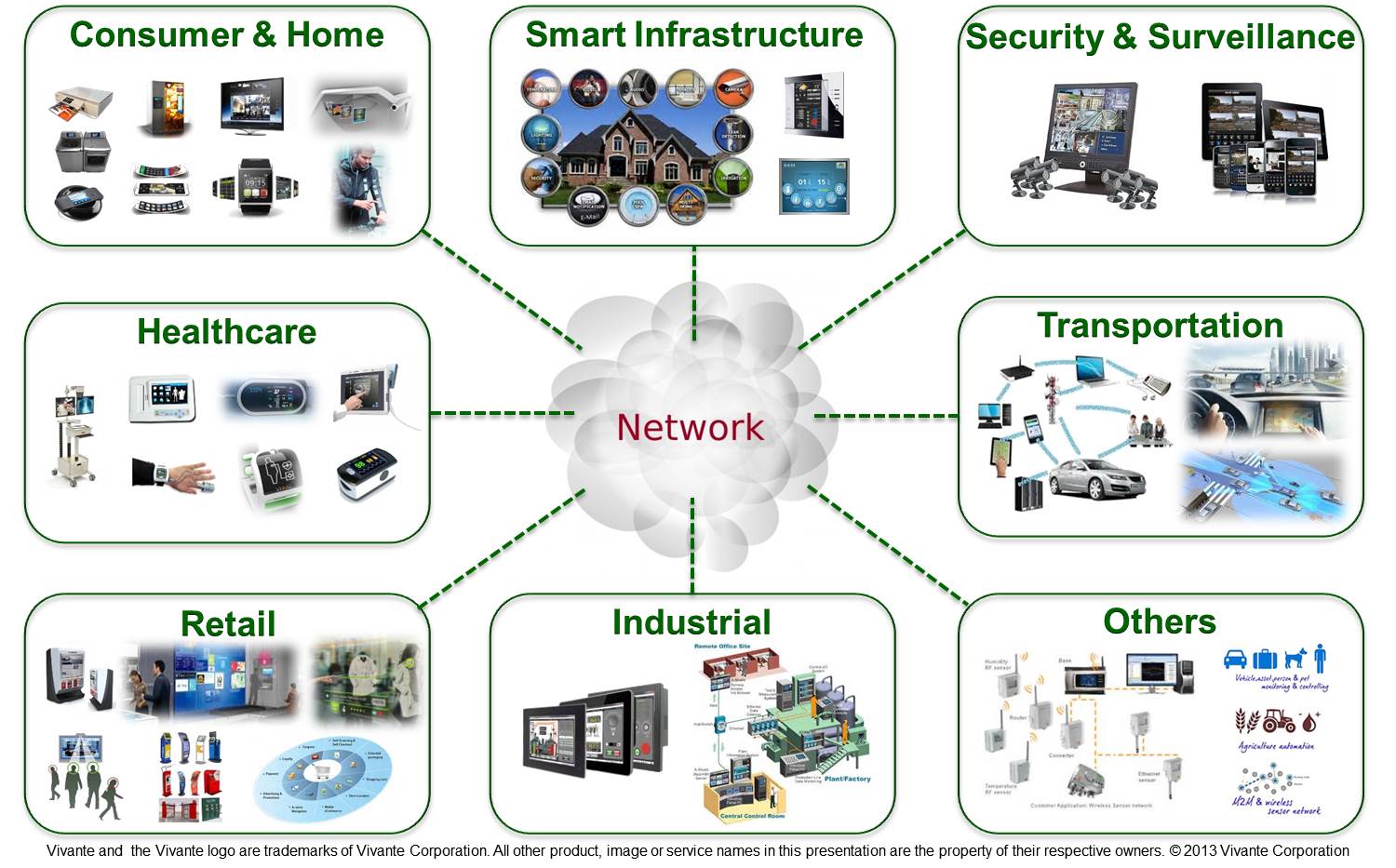
All these areas have interesting applications and many require a consumer friendly display interface that needs to be rendered by a 3D GPU or composition processing core (CPC).
Android as the Backbone of IoT
Android is synonymous with smartphones, tablets, smart TVs, and embedded platforms inside the home, office, automobile, and embedded world, and it can be found pretty much everywhere. In a technology article by Bloomberg Businessweek Technology appropriately titled “Behind the ‘Internet of Things’ Is Android – and It’s Everywhere” it states:
“Android is becoming the standard operating system for the “Internet of Things”—Silicon Valley’s voguish term for the expanding interconnectedness of smart devices, ranging from sensors in your shoe to jet engine monitors…Every screen variant, mobile chip, and sensor known to man has been tuned to work with Android.”
What makes Android a solid platform goes beyond its existing market penetration and its rapidly growing marketshare. It has all the qualities, next generation features, and roadmap needed to support the vast amount of web interconnected products imaginable, including security, upgraded communications protocols, interoperability, and more. From a GPU perspective, the key with using Android to its fullest potential is allowing the visual centric nature of the OS to take center stage. This requires a tiny, IoT based GPU that is full featured and capable of driving the device screen, and a product with a fancier interface will be more enticing to buyers than those without.
As an example, (and assuming costs of both products are similar, which will be the case since a Vivante GPU takes up minimal die area) which device would you like to have? Pre-Android or the Android IoT devices?

About Vivante IoT GPU Products
Optimized for Google Android, Windows Embedded, and other operating systems, Vivante’s IoT product portfolio includes performance-leading technologies in 3D graphics, CPC composition processors, vector graphics, and optional GPGPU cores. Vivante IoT cores leverage a unified driver architecture that is compatible with industry-standard application programming interfaces like OpenGL® ES 2.0, desktop OpenGL®, OpenCL®, OpenVG®, Microsoft® DirectX® 11, WebGL, Google Renderscript / FilterScript Compute, and other standard APIs.
Robust features built into Vivante IoT GPUs include:
- Option 1 (GC400 Core): World’s smallest licensable OpenGL ES 2.0 GPU Core at less than 1 mm2 total silicon area (TSMC 28nm HPM process technology)
- Option 2 (GC880 Core): World’s smallest licensable OpenGL ES 3.0 GPU Core at 2 mm2 total silicon area (TSMC 28nm HPM process technology)
- Supports up to 720p @ 60 FPS with high quality 32-bit color formats (GC400)
- Supports up to 1080p @ 30/60 FPS with high quality 32-bit color formats (GC880)
- Supports all major IoT operating systems, APIs and middleware
- Accelerated composition processing for butter smooth UIs
- Ultra-low power consumption to conserve battery power on-the-go
- Tiny software driver footprint for DDR constrained and DDR-less configurations
- Real-time sensor fusion processing to reduce bandwidth and increase device intelligence
- Industrial temperature support for -40C to 85C
Please visit here for more information on IoT products.
Introducing Vega…the latest, most advanced GPUs from Vivante
By Benson Tao
Breaking News…
One of the latest headlines coming out of IDF 2013 in San Francisco today is the unveiling of a next generation GPU product line from Vivante. This technology continues to break through the the limits of size, performance, and power to help customers deliver unique products quickly and cost-effectively. The first generation solutions were introduced in 2007 (Generation 1) and upgraded again in 2010 (Generation 2) with new enhancements that were shipped in tens of millions of products. Gen 2 solutions already exceeded PC and console quality graphics rendering, which is the standard other GPU IP vendors strive to reach today. The next version (Gen 3) successfully hit key industry milestones by becoming the first GPU IP product line to pass OpenCL™ 1.1 conformance (CTS) and the first IP to be successfully designed into real time mission critical Compute applications for automotive (ADAS), computer vision, and security/surveillance. The early Gen 3 cores, designed and completed before the OpenGL ES 3.0 standard was fully ratified, were forward looking designs that have already passed OpenGL ES 3.0 conformance (CTS) and application testing. Many of the latest visually stunning games can be unleashed on the latest Gen 3 hardware found in leading devices like the Samsung Galaxy Tab 3 (7″), Huawei Ascend P6, Google Chromecast, GoogleTV 2.0/3/0, and other 4K TVs.
With the unveiling of Vivante’s fourth generation (codenamed “Vega”) ScalarMorphic architecture, the latest designs provide a foundation for Vivante’s newest series of low-power, high-performance, silicon-efficient GPU cores. Vivante engineering continues to respond quickly to industry developments and needs, and continuously refines and enhances its hardware specifications in order to remain at the top of the industry through partnerships with ecosystem vendors.
 Sample of Vivante Powered Products
What is Vega?
Vega is the latest, most advanced mobile GPU architecture from Vivante. Leveraging over seven years of architectural refinements and more than 100 successful mass market SOC designs, Vega is the cumulation of knowledge that blends high performance, full featured API support, ultra low power and programmability into a single, well defined product that changes the industry dynamics. SOC vendors can now double graphics performance and support the latest API standards like OpenGL ES 3.0 in the same silicon footprint as the previous generation OpenGL ES 2.0 products. Silicon vendors can also leverage the Vega design to achieve equivalent leading edge silicon process performance in a cost effective mainstream process. This effectively means that given the same SOC characteristics, a TSMC 40nm LP device can compete with a TSMC 28nm HPM version, at a more affordable cost that opens up the market to mainstream silicon vendors that were initially shut out of leading edge process fabrication due to their high initial costs.
Vega is also optimized for Google™ Android and Chrome products (but also supports Windows, BB OS and others), and fast forwards innovation by bringing tomorrow’s 3D and GPU Compute standards into today’s mass market products. Silicon proven to have the smallest die area footprint, graphics performance boost, and scalability across the entire product line, Vega cores extend Vivante’s current leadership in bringing all the latest standards to consumer electronics in the smallest silicon area. Vega 3D cores are adaptable to a wide variety of platforms from IoT (Internet-of-Things) and wearables, to smartphones, tablets, TV dongles, and 4K/8K TVs.
Whether you are looking for a tiny single shader stand-along 3D core or a powerhouse multi-core multi-shader GPU that can deliver high performance 3D and GPGPU functionality, Vivante has a market-proven solution ready to use. There are several options available when it comes to 3D GPU selection: 3D only cores, 3D cores designed with an integrated Composition Processing engine, and 3D cores with full GPGPU functionality that blend real-life graphics with GPU Compute. Vivante already is noted in the industry as the IP provider with the smallest, full-featured licensable cores in every GPU class.
Now let’s dive into some of the Vega listed features to see what they mean…
Hardware Features
- ScalarMorphic™ architecture
- Optimized for multi-GPU scalability and multi-threaded, multi-core heterogeneous platforms. This makes the GPU and GPU Compute cores as independent or cohesive as needed, flexible and developer friendly as new applications built on graphics + compute come online.
- The same premium core architecture as previous generations is still intact, but it has been improved over time to remove inefficiencies. This also allows the same unified driver architecture to work with Vega cores and previous GC cores, so there is no waste of previous developer resources to re-code or overhaul apps for each successive Vivante GPU core.
- Advanced scheduler and command dispatch unit for optimized shader load balancing and resource allocation.
- Dynamic branching and non-constant varying indexing.
- Ultra-threaded, unified shaders
- Maximize graphics throughput, process millions of threads in parallel, and minimize latency.
- The GPU scheduler and cores can process other threads while waiting for data to return from system memory, hiding latency and ensuring the cores are being used efficiently with minimal downtime. Context switching between threads is done automatically in hardware which costs zero cycles.
- These shaders are more than just single way pipelines with added features that make the GPU more general purpose with multi-way pipelines to benefit various processing required for graphics and compute.
- Patented math units that work in the Logarithmic space
- In graphics there are different methods to calculate math and get the correct results. With this method Vega cores can reduce area, power, and bandwidth that speeds up the overall system performance.
- Fast, immediate hidden surface removal (HSR)
- Eliminates render processing time by an average of 30% since a more advanced method to remove back-facing or obscure surfaces is implemented on the fly so minimal or no pre-processing time is wasted. This also goes beyond past versions where the GPU was automatically removing individual pixels (ex. early Z, HZ, etc.).
- Power savings
- Saves power up to 65% over previous GC Cores using intelligent DVFS and incremental low power architectural enhancements.
- Proprietary Vega lossless compression
- Reduces on-chip bandwidth by an average of 3.2:1 and streamlines the graphics subsystem including the GPU, composition co-processsor (CPC), interconnect, and memory and display subsystems. This is important to make sure the entire visual pipeline from when an app makes an API call to the output on the screen is smooth and crisp at optimal frame rates, with no artifacts or tearing regardless of the GPU loading.
- Built-In Visual Intelligence
- ClearView image quality – Life-like rendering with high definition detail, MSAA, and high dynamic range (HDR) color processing. This improves image quality, clarity, and matches real life colors that are not oversaturated.
- Large display rendering – Up to 4K/8K screen resolution including multi-screen support that makes sure the GPU pipelines are balanced.
- New additions using color correction can be implemented to correct color, increase color space using shaders (or OpenCL/RS-FS) or FRC.
- NUIs can also take advantage of visual processing for motion and gesture.
- Industry’s smallest graphics driver memory footprint
- For the first time, smaller embedded or low end consumer devices and DDR-cost constrained systems can now support the latest graphics and various compute applications that fit those segments. With a smaller footprint you don’t need to increase system BOM cost by adding another memory chip, which is crucial in the cost sensitive markets.
- There are also Vivante options that support DDR-less MCU/MPUs in the Vega series where no external DDR system memory exists.
More About the Shaders
- Dynamic, reconfigurable shaders
- Pipelined FP/INT double (64-bit), single/high (32-bit) and half precision/medium (16-bit) precision IEEE formats for GPU Compute and HDR graphics.
- Multi-format support for flexibility when running compute in a heterogeneous architecture where coherency exists between CPU-GPU, high precision graphics, medium precision graphics, computational photography, and fast approximate calculations needed for fast, approximate calculations (for example, some image processing algorithms only need to approximate calculations for speed instead of accuracy). With these options, the GPU has full flexibility to target multiple applications.
- High precision pipeline with support for long instructions.
- Gigahertz Shaders
- Updated pipeline enables shaders to run over 1 GHz, while lowering overall power consumption.
- The high speed along with intelligent power management allows tasks to finish sooner and keep the GPU in a power savings state longer, so average power is reduced.
- Cores scalable from tens of GFLOPS to over 1 TFLOP in various multi-core GPU versions.
- Stream-Out Geometry Shaders
- Increases on-chip GPU processing for realistic, HDR rendering with stream-out and multi-way pipelines.
- The GPU is more independent when using GS since it can process, create and destroy vertices (and perform state changes) without taking CPU cycles. Previous versions required the CPU to pre-process and load states when creating vertices.
Application Programming Interface (API) Overview
Some of the APIs supported by Vega are listed below. This is not an exhaustive list but includes the key APIs in the industry and show the flexibility of the product line.
- Full featured, native graphics API support includes:
- Khronos OpenGL ES 3.0/2.0, OpenGL 3.x2.x, OpenVG 1.1, WebGL
- Microsoft DirectX 11 (SM 3.0, Profile 9_3)
- Full Featured, native Compute APIs and support:
- Khronos OpenCL 1.2/1.1 Full Profile
- Google Renderscript/Filterscript
- Heterogeneous System Architecture (HSA)
Product Line Overview
Please visit the Vivante homepage to find more information on the Vega product line.
- GC400L – Smallest OpenGL ES 2.0 Core – 0.8 mm2 in 28nm
- GC880 – Smallest OpenGL ES 3.0 Core – 2.0 mm2 in 28nm
| GC400 Series | GC800 Series | GC1000 Series | GC2000 Series | GC3000 Series | GC4000 Series | GC5000 Series | GC6000 Series | GC7000 Series | ||
|---|---|---|---|---|---|---|---|---|---|---|
| Vega-Lite | Vega 1X | Vega 2X | Vega 4X | Vega 8X | ||||||
| Core Clock in 28HPM (WC-125) MHz | 400 | 400 | 800 | 800 | 800 | 800 | 800 | 800 | 800 | |
| Shader Clock in 28HPM (WC-125) MHz | 400 | 800 | 1000 | 1000 | 1000 | 1000 | 1000 | 1000 | 1000 | |
| Pixel Rate (GPixel/sec, no overdraw) |
200 | 400 | 800 | 1600 | 1600 | 1600 | 1600 | 3200 | 6400 | |
| Triangle Rate (M tri/sec) |
40 | 80 | 123 | 267 | 267 | 267 | 267 | 533 | 1067 | |
| Vertex Rate (M vtx/sec) |
100 | 200 | 500 | 1000 | 1000 | 2000 | 2000 | 4000 | 8000 | |
| Shader Cores (Vec 4) High/Medium Precision |
1 | 1 | 2 | 4 | 4/8 | 8 | 8/16 | 16/32 | 32/64 | |
| Shader GFLOPS High/Medium Precision |
3.2 | 6.4 | 16 | 32 | 32/64 | 64 | 64/128 | 128/256 | 256/512 | |
| API Support | ||||||||||
| OpenGL ES 1.1/2.0 | ✓ | ✓ | ✓ | ✓ | ✓ | ✓ | ✓ | ✓ | ✓ | |
| OpenGL ES 3.0 | – | Optional | Optional | ✓ | ✓ | ✓ | ✓ | ✓ | ✓ | |
| OpenGL 2.x Desktop | ✓ | ✓ | ✓ | ✓ | ✓ | ✓ | ✓ | ✓ | ✓ | |
| OpenVG 1.1 | ✓ | ✓ | ✓ | ✓ | ✓ | ✓ | ✓ | ✓ | ✓ | |
| OpenCL 1.2 | – | Optional | Optional | ✓ | ✓ | ✓ | ✓ | ✓ | ✓ | |
| DirectX11 (9_3) SM3.0 | – | Optional | Optional | ✓ | ✓ | ✓ | ✓ | ✓ | ✓ | |
| Key: ✓ (Supported) – (Not supported) | ||||||||||
Join us @ Khronos BoF Day (SIGGRAPH 2013)
Exciting new things being presented at the Khronos BoF today. You will learn about the new camera WG and Camera API initiatives happening that take advantage of OpenCL, OpenGL ES, OpenVX, and StreamImput. The trend went from traditional photography to computational photography, and now, to perceptual photography (this is a new term that came up today). Improving HDR images (quality, range, bandwidth, memory footprint, computational loading, etc.) is an exciting application where the Khronos group is heading. Multi-sensor applications (ex. Pelican Imaging), stereo, dynamic effects, etc., even though in its infancy as a mainstream technology, is now being pushed hard by the industry. With the inclusion of GPUs in the computational (imaging) pipeline new image dynamics are constantly being enabled to enhance the user experience.
New updates in OpenGL/GL ES will be given throughout the day as we take a look at the GLES 3 and the next generation graphics API. This is also an exciting time as it marks the 10th anniversary of OpenGL ES.
Please join us at the Khronos BoF event so we can update you on the latest information.
Event: Khronos BoF Date: July 24th Time: All Day Location: Anaheim Hiliton (California Ballroom, 2F)
Exciting Updates @ SIGGRAPH 2013 HSA BoF
Please join us at the Heterogeneous System Architecture (HSA) Foundation’s BoF (Bird of Feather) talk at SIGGRAPH 2013. Phil Rogers, President of HSA and AMD Fellow will give the keynote speech and update us on the exciting progress they have made to push the standard and technology forward. The BoF session will also have a Q&A section where you can get answers to some of your toughest questions.
Please look for us when you are there to ask us how we are innovating in this area, or you can just say “Hello” to us.
Event: HSA Foundation BoF Date: July 24th Time: 1 pm Location: Anaheim Convention Center ( Room 202 B)
Huawei Ascend P6 Smartphone…Thin, Sexy, and Intuitive
By Benson Tao (Vivante Corporation)
The rise of Huawei is a corporate success story (and MBA case study) of determination and will to do whatever it takes to make a difference in people’s lives. This goal is achieved through the creation of the best and most innovative products possible without cutting corners or taking short cuts. This perseverance has turned Huawei from a tiny company that started selling PBX (private branch exchange or telephone switches) to a global behemoth that recently rose to take the crown as the world’s largest telecoms equipment maker in the world, surpassing Ericsson last year. The rapid rise of Huawei has also made it one of the top global brands in the world and a household name in some parts of the world. As the 2010 Fast Company fifth most innovative company in the world, a natural extension of their product line was to develop cutting edge smartphones and tablets to complement their existing user and communications infrastructure base. In the past year, their fruits of labor have helped push the mobile market forward with a few leading (and surprising) innovations:
- Fastest Quad core smartphone (Ascend Quad D)
-
One of the first 1080p smartphones (Ascend Quad D2)
-
World’s fastest LTE smartphone (Ascend P2)
-
…AND the just announced thinnest smartphone in the world measuring only 6.18 mm thick (Ascend P6)

Ascend P6 (Source: Huawei)
What do all these leading Huawei products have in common, other than all being branded under the Ascend name? At the heart of each product is one of the best architected Quad Core CPU and GPU combinations the market has seen, all packaged in a Hisilicon K3V2 SoC. Hisilicon is the semiconductor division of Huawei and is one of the suppliers of products to their systems division that defines or builds final products. Huawei can source product from Hisilicon, Qualcomm, and others to fit product requirements (cost, performance, low power, etc.).
One reason the K3V2 was chosen to power their flagship phones was the capability, scalability, extreme low power, and performance of the Vivante GC4000 (Graphics and Compute) GPU. Extensive due diligence to qualify the Vivante architecture was done under a microscope to make sure the GPU could meet all relevant claims. In the end, the GC4000 met or exceeded the demanding test criteria for 3D graphics performance to play the most intense and detailed mobile 3D games, and the Vivante CPC (Composition Processing Core) helped accelerate their intuitive Emotion UI user interface for responsive, smooth, and fluid feedback.


Source: Huawei
The Ascend P6 is the best and most beautiful smartphone Huawei has designed, with intricate details going into its amazing design (look), high quality materials, metallic body (feel), and ease of use. For more information about the Ascend P6, please visit their minisite.

Images (and Pixels)…The Next Generation Hyperlink
By Benson Tao (Vivante Corporation)
Background
The world is very visual and thanks to the popularity of media processors (GPUs and VPUs), multimedia has become a ubiquitous part of life. Most of the things we interact with have some sort of screen, ranging from the usual consumer products to washing machines, thermostats, and any other product or gadget that needs to be upsold. Stick a screen on something, maybe add a camera, install Android, and you have a device that could be part of your Internet of Things (IoT) which you can probably sell for a premium…before the next product comes out the next day.
With the rise of multimedia that is standard across all screened devices, so has the explosive growth of media exchange that includes pictures, images, and videos. YouTube has 100 hours of video content uploaded every minute! Facebook has 250 million photos uploaded daily and over 100 billion (as of 2011) photos on its servers! These huge numbers have so many zeroes and something never seen before, and each day those numbers get larger and larger. The rise of visual media content is great, you can find clips of cats playing pianos, live, courtside highlights from the NBA playoffs, and pretty much anything that catches your attention. The flipside of the story is – How do you search for content without getting lost in the noise? Just going through links to find what you want can take a few seconds for simple, straightforward queries, to several minutes or hours for more involved searches. But this number is rising due to the massive amounts of data, and getting relevant search results fast is what counts. As more searches involve multimedia, text hyperlinks will not work so a new generation of visual search (as the new hyperlink) will become standard. QR codes tried to be different, but those have not been successful.
From a high level, VS/MVS is a way of interacting with the world around you. Those interactions can take the form of video, graphics or audio. Bits of these technologies are available, it’s just a matter of packaging them together in the most efficient way. As an example, there are apps that can “listen” to a song and tell you what it is (Shazam is one example). Google Googles is also capable of MVS. In general, a device takes a picture of an image and the image (ex. JPEG) is sent over the network to a server that compares the image and tries to return an answer. Different methods to reduce the transmission and response time have been used where pre-processing is done on the smartphone which reduces the search window to a smaller subset and possibly eliminates server interaction for some use cases.
GPUs in VS/MVS
This is where visual search or mobile visual search comes into play and where the GPU inside a smartphone/tablet or TV applications processor plays in the next generation of search. We have seen PC GPUs play an important role in identifying faces in photos (visual search) using OpenCL with software from Cyberlink or Corel that can identify and sort photos based on different queries. You can search for all photos with John Doe and the GPU searches through the image database and returns all photos with John Doe (assuming he doesn’t have a had and sunglasses on). The results are pretty good, not perfect, but nothing that has this much complexity is perfect in the real world.
Fast forward to today…mobile GPUs have lots of horsepower packed into such die area constrained designs that if not used, it just sits there idle and you remove the efficiency (and potential) of what the technology can do. Many groups are researching how to add mobile visual search optimizations to GPUs like those at Vivante, and the push forward will improve implementations in augmented reality (AR), GPU accelerated MVS, vision processing (can include automotive, consumer electronics, etc.) and many other applications.
The idea of using the GPU has a few areas of consideration:
-
Bandwidth efficiency – Compression or pre-computations on the device to minimize server-client transmissions. Part of this also involves network latency and possibly lower quality image if there are transmission limitations.
- Lower Power / Thermals on Servers Side – Servers need to compare an image vs. a database, which takes a lot of computational workload.
- Lower Power / Thermals on Client Side – GPUs are fast and efficient when dealing with parallel workloads. Many search algorithms use parallel computations which are best suited for the GPU.
- Higher Quality VS/MVS Results – Search results can scale with the GPU with increased accuracy (since GPUs are good at image/pixel processing).
MPEG Group Visual Search Development
I recently saw a new specification developed by the folks at MPEG or Motion Picture Experts Group related to Visual Search (Compact Descriptors for Visual Search) and this is an exciting topic where GPU technology can make it shine. If you have not heard of MPEG, they are responsible for creating the video/audio transmission standards used pretty much by whatever video content you watch. Things like MP3 (audio), MPEG-2, MPEG-4, H.264, and HEVC have all come from that consortium. Since they are the 800 lbs gorilla when it comes to video, they want to create a standard VS/MVS solution that will be interoperable across any device and platform and efficient (bandwidth, algorithm computational overhead, etc.). This is great news since a fragmented solution can break a superb idea, and Khronos is looking at how they can cooperate with MPEG to see how it can play a role in future APIs. This should open up the doors for exciting new applications on any device.
